Choosing the wrong semiconductor packaging leads to costly delays, wasted resources and compromised reliability, but how do lead frame package compare to substrate solutions? For semiconductor professionals, this guide covers all key details about lead frame packages from structure and manufacturing to types and substrate comparisons to help you avoid errors and make confident, cost-effective decisions.
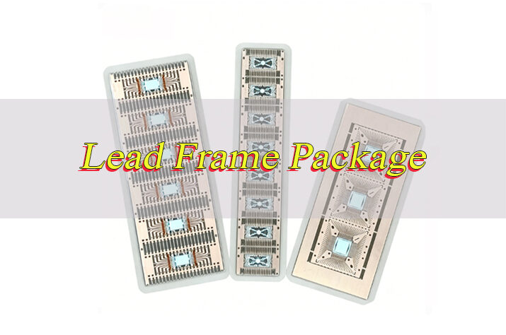
What is a Lead Frame Package (LFP) in Semiconductor Manufacturing?
A lead frame package is a semiconductor packaging solution that uses a metal frame to connect the internal chip to external circuitry. It serves as the bridge between the semiconductor die and the printed circuit board, facilitating electrical signal transmission, providing physical support for the chip, and protecting the die from environmental damage such as moisture and dust.
Unlike more complex packaging solutions, lead frame packages rely on a simple, cost effective design that makes them ideal for a wide range of low to mid complexity semiconductor devices. They are widely used in consumer electronics, automotive components, and industrial equipment, where reliability and cost efficiency are top priorities.
The core function of a lead frame package is to route electrical signals from the chip’s bond pads to the external leads, which are then soldered to the PCB. This connection ensures the chip can communicate with other components in the system, while the package itself shields the die from mechanical stress and environmental hazards that could degrade performance or cause failure.
What are the Components of a Lead-Frame Package Structure?
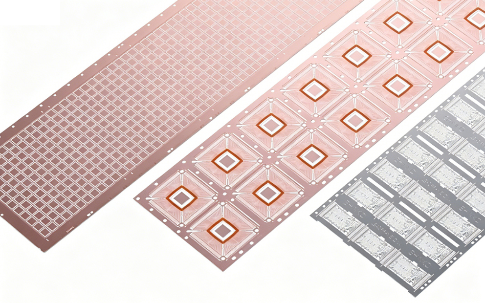
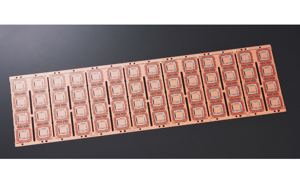
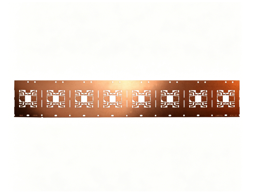
A lead frame package consists of several key components that work together to ensure reliable performance and protection. Each component has a specific role, and any defect in these parts can lead to package failure or reduced functionality.
| Component | Description | Function |
|---|---|---|
| Lead Frame | Thin metal sheet (typically copper or copper alloy) with precision-cut leads and a die pad | Supports the die, routes electrical signals, and dissipates heat from the chip |
| Semiconductor Die | The core semiconductor chip that contains the active circuitry | Performs the primary electrical function of the device (e.g., amplification, switching) |
| Die Attach Material | Adhesive (epoxy, silver paste, or solder) that bonds the die to the lead frame’s die pad | Secures the die in place, provides thermal conductivity, and ensures electrical isolation where needed |
| Wire Bonds | Thin metal wires (gold, copper, or aluminum) with diameters ranging from 15-50 μm | Connect the die’s bond pads to the lead frame’s inner leads, enabling signal transmission |
| Mold Compound | Epoxy-based thermosetting material that encapsulates the die, wire bonds, and inner leads | Protects internal components from moisture, dust, mechanical stress, and chemical damage |
| External Leads | Extended portions of the lead frame that extend outside the mold compound | Connect the lead frame package to the PCB, enabling electrical connection to the larger system |
What Materials are Used for Lead Frame Packaging and Why?
Selecting the right materials for lead frame packaging is critical to its performance, reliability and cost-effectiveness. Key factors like electrical conductivity, thermal performance, cost and manufacturing compatibility directly impact how well the package serves its intended use. Below, we break down the most common materials for lead frame packaging, including their properties, advantages and ideal use cases.
- Copper and Copper Alloys: The most common lead frame materials. Copper has excellent electrical and thermal conductivity, ideal for high-power chips. Alloys like Cu-Ni-Si and Cu-Sn boost mechanical strength and corrosion resistance, widely used in automotive and industrial applications requiring durability.
- Gold: Primarily used for wire bonds, offering superior conductivity, corrosion resistance and bond reliability. It is ideal for high-reliability applications like medical devices and aerospace, with easier manufacturability to reduce bond failure risk.
- Aluminum: A cost-effective alternative to gold for wire bonds, with good conductivity. It is widely used in consumer electronics and compatible with high-volume manufacturing.
- Epoxy Mold Compounds: Thermosetting materials that encapsulate the die and wire bonds, providing protection against moisture and mechanical stress. They offer good thermal stability and electrical insulation, with formulations for diverse applications including high-temperature automotive use.
- Die Attach Epoxy: Bonds the die to the lead frame’s die pad, with high thermal conductivity to prevent overheating and strong adhesion. Silver-filled epoxies are used for high-power devices to enhance thermal performance.
What is the Full Manufacturing Process of a Lead Frame Package?
The manufacturing process of a lead frame package involves several sequential steps, each critical to ensuring the final product meets performance and reliability standards. Following these steps precisely reduces defects and ensures consistent quality across production batches.
Step 1: Lead Frame Fabrication: The process starts with a thin metal sheet (typically copper or copper alloy) that is cut into the desired shape using either stamping or etching. Stamping is used for high volume production, as it is fast and cost effective, while etching is used for more complex lead frame designs with finer pitches. The lead frame is then cleaned and plated with a thin layer of nickel or tin to improve corrosion resistance and solderability.
Step 2: Die Attach: The semiconductor die is attached to the lead frame’s die pad using die attach epoxy or silver paste. The die is carefully placed on the die pad, and the assembly is heated to cure the adhesive. This step ensures the die is securely bonded and that heat can transfer efficiently from the die to the lead frame.
Step 3: Wire Bonding: Thin metal wires (gold, aluminum, or copper) are used to connect the die’s bond pads to the lead frame’s inner leads. This is done using either ultrasonic bonding or thermosonic bonding, which creates a strong, reliable electrical connection. The wire bonds must be precisely placed to avoid short circuits and ensure optimal signal transmission.
Step 4: Molding: The die, wire bonds, and inner leads are encapsulated in an epoxy mold compound. The assembly is placed in a mold, and the mold compound is injected under high pressure and temperature. The compound cures to form a protective shell around the internal components, shielding them from environmental damage.
Step 5: Post Mold Cure: After molding, the package is heated in an oven to fully cure the mold compound. This step improves the mechanical strength and thermal stability of the package, ensuring it can withstand the stresses of subsequent manufacturing steps and application use. The post mold cure typically takes 8-12 hours at temperatures between 150-175°C.
Step 6: Lead Trimming and Forming: The external leads of the lead frame are trimmed to the desired length and bent into the appropriate shape (e.g., J lead, gull wing). This step ensures the leads can be easily soldered to the PCB and fit within the device’s form factor. Precision trimming and forming are critical to avoid lead damage and ensure consistent lead geometry.
Step 7: Plating: The external leads are plated with a thin layer of tin, tin lead, or gold to improve solderability and corrosion resistance. Tin plating is the most common, as it is cost effective and compatible with most soldering processes. The plating thickness is carefully controlled to ensure optimal performance.
Step 8: Testing and Inspection: The finished lead frame packages are tested for electrical performance, including continuity, insulation resistance, and functionality. They are also inspected for physical defects such as mold cracks, wire bond failures, and lead damage. Packages that fail testing are discarded, while those that pass are prepared for packaging and shipment.
What are the Most Common Types of Lead Frame Packaging for Electronics?
Lead frame packages come in various types, each designed for specific applications and chip requirements. The choice of package type depends on factors such as the number of I/O pins, chip size, power requirements, and form factor constraints.
- Dual In Line Package (DIP): One of the oldest and most common lead frame package types. DIP packages have leads on both sides of the mold, arranged in a straight line. They are available in plastic or ceramic versions and are widely used in through hole mounting applications. DIP packages are ideal for low pin count devices (4-40 pins) such as logic gates and voltage regulators.
- Small Outline Package (SOP): A surface mount lead frame package with leads on two sides, bent into a gull wing shape. SOP packages are smaller than DIP packages, making them suitable for compact electronic devices such as smartphones and tablets. They are available in various sizes, including SOIC (Small Outline Integrated Circuit) and SSOP (Shrink Small Outline Package), and support pin counts from 8-48.
- Quad Flat Package (QFP): A surface mount package with leads on all four sides, bent into a gull wing shape. QFP packages support higher pin counts (44-208 pins) than SOP packages, making them suitable for more complex devices such as microcontrollers and ASICs. They are widely used in automotive and industrial applications where high I/O count is required.
- Plastic Leaded Chip Carrier (PLCC): A square surface mount package with J shaped leads on all four sides. PLCC packages have a cavity in the center where the die is mounted, providing excellent protection for the chip. They are used in applications where space is limited and high reliability is required, such as medical devices and aerospace components.
- TO Package (Transistor Outline): A lead frame package designed specifically for discrete components such as transistors, diodes, and voltage regulators. TO packages have a metal case (for high power devices) or plastic case (for low power devices) and a small number of leads (2-6). They are widely used in power electronics and industrial applications.
- Chip Scale Package (CSP) Lead Frame Variant: A compact lead frame package where the package size is nearly the same as the die size. These packages are used in ultra compact devices such as wearables and smartphones, where space is at a premium. They support high pin counts and offer excellent thermal performance.
Is a Stacked Chip Scale Package (SCSP) a Type of Lead Frame Package?
No, a Stacked Chip Scale Package (SCSP) is not a type of lead frame package. SCSP is a advanced packaging solution that belongs to the substrate based packaging category, not the lead frame based category.
SCSP is designed to stack multiple chips vertically in a single package, reducing the overall footprint and increasing integration density. This is achieved using a substrate (typically a thin, high density interposer) to connect the stacked chips, rather than a metal lead frame. The substrate provides finer pitch interconnections between the chips, enabling higher I/O density and better signal integrity.
While some SCSP variants may use lead frame like components for external connections, the core structure of SCSP relies on a substrate, not a lead frame. This distinction is critical for professionals selecting packaging solutions, as substrate based packages like SCSP are better suited for high density, high performance applications, while lead frame packages are ideal for cost sensitive, low to mid complexity devices.
Another key difference is that SCSP supports vertical stacking of multiple chips, which is not feasible with traditional lead frame packages. Lead frame packages are typically designed for a single chip, although some variants can accommodate multiple chips in a side by side arrangement. SCSP’s vertical stacking capability makes it ideal for applications such as memory modules and high performance SoCs (System on Chips).
What Should Be Considered in Lead Frame Package Design?
Designing a lead frame package requires careful consideration of multiple factors to ensure optimal performance, reliability, and manufacturability. Below are the key design considerations:
- Pin Count and Pitch: The number of I/O pins and their pitch must match the chip’s requirements and PCB design. Lead frame packages are practical for 4-200 pins; exceeding 200 pins increases complexity and defects. Standard lead pitches range from 0.5 mm to 1.27 mm (0.5 mm minimum), with finer pitches requiring more costly etching. Low pin count devices suit DIP packages, while mid-range pin counts require QFP packages to avoid lead overcrowding and signal interference.
- Thermal Management: The package must efficiently dissipate chip heat. Copper lead frames offer superior thermal conductivity, while optimizing die pad size and adding thermal vias enhance heat dissipation. High-power devices benefit from integrated copper heat sinks to prevent overheating.
- Mechanical Stress: The package must withstand manufacturing and application stress, especially thermal cycling. Lead frames need sufficient tensile strength (copper alloys like Cu-Ni-Si are suitable), while mold compound and die attach materials should match the chip’s CTE to prevent cracking and delamination.
- Electrical Performance: Lead frame design must minimize signal delay, crosstalk, and EMI. Optimizing lead length and spacing reduces interference, while shielded leads and proper grounding are critical for EMI-sensitive applications.
- Manufacturability: The design must be compatible with standard processes (stamping, etching, wire bonding) to avoid extra costs. Stamping is ideal for high-volume production, while etching suits complex designs. Using standard wire diameters ensures high bond yield and reduces rework.
- Environmental Requirements: The package must withstand the target application’s environment. Automotive packages meet AEC-Q100 standards, industrial packages resist moisture per IPC-6012, and medical packages use biocompatible materials and withstand sterilization.
- Cost: Balance performance and cost by choosing appropriate materials and designs. Copper lead frames and aluminum wire bonds reduce costs for consumer electronics, while gold bonds are worthwhile for high-reliability applications. High-volume production lowers unit costs.
- PCB Compatibility: External leads must match PCB mounting technology. SMT leads use gull wing or J shapes, while through-hole leads have specific diameters. Precise lead length tolerance ensures consistent soldering.
- Reliability Standards: The package must meet industry standards (JEDEC JESD47, IPC-6012, IPC-610) to ensure field performance and reduce failure rates, protecting brand reputation and warranty costs.
What are the Advantages and Limitations of Lead Frame Packaging?
Lead frame packages offer several key advantages that make them a popular choice for many semiconductor applications, but they also have limitations that restrict their use in certain high performance or high density scenarios.
Advantages of Lead Frame Packaging:
- Cost Effective: Lead frame packages are simpler to manufacture than substrate based packages, resulting in lower production costs. This makes them ideal for cost sensitive applications such as consumer electronics.
- High Reliability: The simple design and robust materials used in lead frame packages make them highly reliable, even in harsh environments. They are resistant to mechanical stress, moisture, and temperature extremes.
- Good Thermal Performance: Copper lead frames offer excellent thermal conductivity, allowing for efficient heat dissipation from the chip. This is critical for high power devices that generate significant heat.
- Easy to Manufacture: Lead frame packages can be produced using standard manufacturing processes (e.g., stamping, wire bonding) that are widely available and well established. This enables high volume production with consistent quality.
- Wide Compatibility: Lead frame packages are compatible with a wide range of chip sizes, pin counts, and PCB mounting technologies. They can be used for both through hole and surface mount applications.
Limitations of Lead Frame Packaging:
- Limited Pin Count: Lead frame packages are not suitable for high pin count devices (above 200 pins) due to space constraints. Substrate based packages are better suited for high I/O density applications.
- Larger Footprint: Compared to substrate based packages such as CSP and BGA, lead frame packages have a larger footprint, making them less suitable for ultra compact devices.
- Finer Pitch Limitations: Lead frame packages have limitations in terms of lead pitch, with the minimum practical pitch being around 0.5 mm. Substrate based packages can achieve finer pitches (down to 0.1 mm), enabling higher integration density.
- Limited Stacking Capability: Traditional lead frame packages are designed for single chip applications, making them unsuitable for stacked chip designs that require vertical integration.
What are the Common Defects in Lead Frame Packaging and How to Avoid Them?
Lead frame packaging can experience several common defects during manufacturing, which can reduce reliability or cause complete package failure. Understanding these defects and how to avoid them is critical to ensuring consistent quality and reducing production costs.
- Wire Bond Failure: This occurs when the wire bond between the die and lead frame fails to form a strong connection. It can be caused by poor wire bonding parameters (e.g., temperature, pressure), contaminated bond pads, or defective wire. To avoid this, ensure bond pads are clean, optimize wire bonding parameters, and use high quality wire materials.
- Mold Cracks: Cracks in the mold compound can occur due to excessive mechanical stress during molding, improper post mold cure, or thermal cycling. To avoid this, use a mold compound with appropriate flexibility, optimize molding parameters (e.g., temperature, pressure), and ensure proper post mold cure to reduce internal stress.
- Die Attach Voiding: Voids in the die attach material can reduce thermal conductivity and mechanical strength, leading to chip overheating and failure. This is caused by air bubbles in the die attach material or improper curing. To avoid this, use die attach materials with low viscosity (to reduce air entrapment) and ensure proper curing temperature and time.
- Lead Damage: Damage to the external leads (e.g., bending, kinking) can occur during lead trimming and forming or handling. This can lead to poor solder joints and electrical connection issues. To avoid this, use precision trimming and forming equipment, handle packages carefully, and ensure proper packaging during shipment.
- Corrosion: Corrosion of the lead frame or wire bonds can occur due to exposure to moisture, chemicals, or harsh environments. This is caused by inadequate plating or poor mold compound sealing. To avoid this, use high quality plating materials (e.g., tin, gold), ensure the mold compound provides a tight seal, and select packages with corrosion resistant materials for harsh environments.
- Short Circuits: Short circuits can occur between wire bonds, leads, or the die and lead frame. This is caused by misaligned wire bonds, excessive mold flash, or contamination. To avoid this, ensure precise wire bond alignment, optimize molding parameters to reduce flash, and maintain a clean manufacturing environment.
Which Industries and Applications Use Lead Frame Packages Most Frequently?
Lead frame packages are widely used across various industries, thanks to their cost efficiency, reliability, and versatility. They are particularly popular in applications where performance requirements are moderate and cost is a key consideration.
- Consumer Electronics: The largest user of lead frame packages, used in smartphones, tablets, laptops and televisions for power management ICs, logic gates, and sensors.
- Automotive: Used in automotive electronics such as ECUs, sensors, and power management devices, with copper lead frames for thermal conductivity and durability.
- Industrial Equipment: Used in industrial controllers, power supplies, and sensors for reliable performance in harsh industrial environments.
- Medical Devices: Used in low to mid complexity medical devices (e.g., blood glucose monitors) with gold wire bonds for high reliability and biocompatibility.
- Power Electronics: Used in power transistors, diodes, and voltage regulators, leveraging copper lead frames for efficient heat dissipation.
- Telecommunications: Used in routers, modems, and communication modules for signal amplifiers and voltage regulators.
What are the Main Differences Between Lead Frame Package and Substrate Package?
Lead frame packages and substrate packages are two distinct semiconductor packaging solutions, each with unique characteristics and applications. Understanding their differences is critical to selecting the right package for a specific device or application.
| Characteristic | Lead Frame Package | Substrate Package |
|---|---|---|
| Core Structure | Uses a metal lead frame to connect the die to external circuitry | Uses a thin substrate (organic or ceramic) with high density interconnections |
| Pin Count | Suitable for low to mid pin counts (up to 200 pins) | Suitable for high pin counts (200+ pins) and high I/O density |
| Footprint | Larger footprint compared to substrate packages | Smaller footprint, ideal for ultra compact devices |
| Lead Pitch | Minimum pitch of ~0.5 mm | Finer pitch (down to 0.1 mm) for higher integration |
| Thermal Performance | Excellent thermal conductivity (copper lead frames) | Good thermal performance, but often requires additional heat sinks |
| Cost | Lower cost, ideal for cost sensitive applications | Higher cost due to complex substrate manufacturing |
| Manufacturability | Simple to manufacture with standard processes | Complex manufacturing requires specialized equipment |
| Applications | Consumer electronics, automotive, industrial equipment, low to mid complexity devices | High performance devices, high I/O density chips, ultra compact devices (e.g., smartphones, wearables) |
| Stacking Capability | Limited, typically single chip or side by side multiple chips | Excellent, supports vertical stacking of multiple chips (e.g., SCSP, 3D ICs) |
FAQs About Lead Frame Packaging
Q1: How long does a lead frame package typically last in automotive applications?
A1: A lead frame package designed for automotive applications typically lasts 10-15 years under normal operating conditions. This lifespan is achieved through the use of durable materials (e.g., copper alloys, corrosion resistant plating) and compliance with automotive reliability standards (JEDEC JESD47). Proper thermal management and environmental sealing further extend the lifespan, even in harsh automotive environments with temperature extremes and vibration.
Q2: Can lead frame packages be used for high power semiconductor devices?
A2: Yes, lead frame packages can be used for high power semiconductor devices. Copper lead frames offer excellent thermal conductivity (401 W/m·K), which allows for efficient heat dissipation from high power chips. Additionally, lead frame packages can be designed with larger die pads and heat sinks to further enhance thermal performance. They are commonly used for power transistors, diodes, and voltage regulators in automotive and industrial applications.
Q3: Are lead frame packages compatible with RoHS and other environmental standards?
A3: Yes, most lead frame packages are compatible with RoHS (Restriction of Hazardous Substances) and other environmental standards. Manufacturers use lead free plating materials (e.g., tin, tin silver) instead of lead tin alloys, and epoxy mold compounds that are free of hazardous substances. Lead frame packages can also be designed to meet other environmental standards, such as REACH and WEEE, making them suitable for global applications.
Q4: How do I choose between a lead frame package and a substrate package for my device?
A4: Choose a lead frame package if your device has low to mid pin counts (up to 200 pins), requires cost efficiency, and does not need an ultra compact footprint. Lead frame packages are ideal for consumer electronics, automotive, and industrial applications where reliability and thermal performance are important but high I/O density is not. Choose a substrate package if your device has high pin counts (200+ pins), requires a small footprint, or needs vertical chip stacking (e.g., high performance SoCs, wearables).
Q5: What is the typical cost of a lead frame package compared to a substrate package?
A5: Lead frame packages are significantly less expensive than substrate packages. On average, a lead frame package costs 30-70% less than a substrate package with similar pin counts. This cost difference is due to the simpler manufacturing process of lead frame packages, which uses standard equipment and materials. Substrate packages are more expensive because they require specialized manufacturing processes for the high density substrate.
Q6: Can lead frame packages be used in surface mount technology (SMT) applications?
A6: Yes, most modern lead frame packages are designed for surface mount technology (SMT) applications. SMT compatible lead frame packages (e.g., SOP, QFP, PLCC) have leads bent into gull wing or J shapes, which allow them to be soldered directly to the surface of the PCB. This eliminates the need for through holes, reducing the PCB size and enabling more compact device designs. Lead frame packages are widely used in SMT applications across consumer electronics, automotive, and industrial industries.
Tags: Lead Frame Package, Lead Frame Package Design, Substrate Package
PakarPBN
A Private Blog Network (PBN) is a collection of websites that are controlled by a single individual or organization and used primarily to build backlinks to a “money site” in order to influence its ranking in search engines such as Google. The core idea behind a PBN is based on the importance of backlinks in Google’s ranking algorithm. Since Google views backlinks as signals of authority and trust, some website owners attempt to artificially create these signals through a controlled network of sites.
In a typical PBN setup, the owner acquires expired or aged domains that already have existing authority, backlinks, and history. These domains are rebuilt with new content and hosted separately, often using different IP addresses, hosting providers, themes, and ownership details to make them appear unrelated. Within the content published on these sites, links are strategically placed that point to the main website the owner wants to rank higher. By doing this, the owner attempts to pass link equity (also known as “link juice”) from the PBN sites to the target website.
The purpose of a PBN is to give the impression that the target website is naturally earning links from multiple independent sources. If done effectively, this can temporarily improve keyword rankings, increase organic visibility, and drive more traffic from search results.