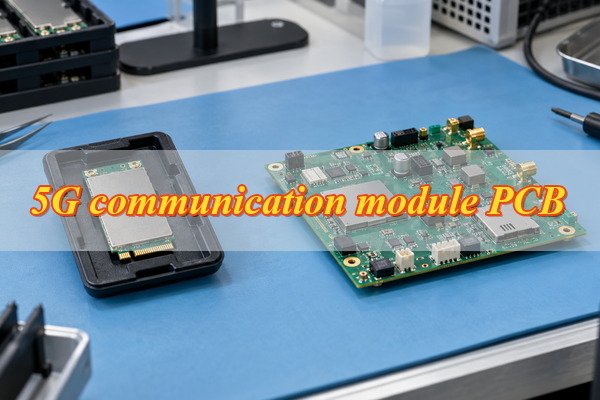
A 5G communication module PCB carries RF signals, distributes power, and links high‑speed digital interfaces in 5G equipment. EBest Circuit manufactures multilayer, HDI, and high‑frequency PCBs and provides component sourcing and PCBA assembly for 5G modules and carrier boards, from prototypes to repeat production.
The manufacturing route changes depending on whether the board sits inside a compact modem or carries a finished module. Impedance control, stackup, fine‑pitch features, module footprints, and thermal management all need to match the approved design. The sections below connect those requirements to fabrication, assembly, testing, lead time, and the files needed for an accurate quotation.
What Is a 5G Communication Module PCB?
A 5G communication module PCB is either the circuit board inside a 5G modem module or a carrier board that connects a finished module to a host system. It supports RF connections, power delivery, and digital communication interfaces.
These boards are used in industrial gateways, 5G routers, IoT terminals, and wireless communication equipment. An internal module PCB may need dense routing and fine‑pitch packages, while a carrier board usually concentrates on module connections, power supply, antenna interfaces, and communication with the host device.
The module architecture determines the manufacturing requirements. Confirm whether the project concerns an internal module PCB or a host carrier board before choosing materials, stackup, footprints, and assembly processes.
What Materials and Stackups Are Used in 5G Communication Module PCBs?
FR-4, high‑Tg FR-4, low‑loss RF laminates, and hybrid stackups can all be used in 5G communication module PCBs. The right choice depends on the frequencies routed on the board, signal‑loss limits, thermal conditions, and layer construction.
| PCB Material | Typical Application | Manufacturing Considerations |
|---|---|---|
| FR-4 | 5G carrier boards and digital interface circuits | Dielectric properties, board thickness, and impedance |
| High‑Tg FR-4 | Multilayer boards requiring greater thermal stability | Glass transition temperature, thermal expansion, and assembly conditions |
| Low‑Loss RF Laminate | High‑frequency RF transmission lines | Dielectric constant (Dk), dissipation factor (Df), and insertion loss |
| Hybrid Stackup | Boards combining RF, digital, and power circuits | Material compatibility, lamination, and dimensional stability |
A 5G carrier PCB does not automatically require a low‑loss RF laminate. FR-4 may be suitable when the module contains the high‑frequency RF circuitry and the carrier board still meets the specified electrical requirements.
The released stackup should state dielectric thickness, copper weight, layer arrangement, and controlled‑impedance requirements. Substituting a laminate without reviewing its dielectric properties can change transmission‑line impedance and insertion loss, so material changes need approval before fabrication.
What Should Be Checked Before 5G Communication Module PCB Fabrication?
Before fabricating a 5G communication module PCB, review the stackup, module footprint, fine‑pitch features, thermal structures, and RF reference geometry against the Gerber files, fabrication drawings, and selected module datasheet.
The main DFM checks include:
- Controlled Impedance: Verify trace dimensions, dielectric thickness, copper weight, and impedance targets. RF antenna connections commonly use 50 Ω transmission lines.
- Fine‑Pitch Features: Check pad dimensions, line spacing, solder mask openings, and assembly clearances against the selected packages.
- Microvias and Via‑in‑Pad: Confirm via dimensions, copper plating, filling, and capping requirements where the design uses these structures.
- Module Footprints: Compare LGA land patterns and M.2 connector footprints with the module manufacturer’s specifications.
- Thermal Structures: Review thermal pads, copper planes, heat‑transfer vias, and mounting requirements.
- RF Grounding and Shielding: Check specified ground structures, via locations, connector launches, and shielding footprints against the approved layout.
LGA and M.2 modules need different assembly plans. An LGA module is soldered to the PCB, while an M.2 module normally plugs into a socket. An incorrect footprint or retention arrangement can make the finished board unusable even when the bare board passes electrical testing.
EBest Circuit provides DFM review and manufacturing guidance, not circuit design. Resolve any conflict among fabrication files, module datasheets, and assembly drawings before production starts.
How Are 5G Communication Module PCBs Manufactured and Assembled?
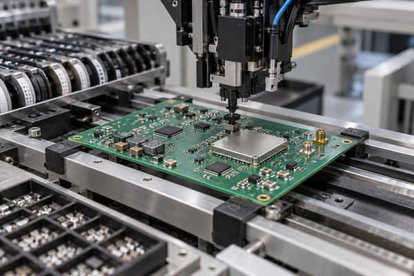
Manufacturing combines PCB fabrication, controlled component sourcing, assembly, and inspection. The exact route depends on the board construction and whether the 5G module is soldered directly to the PCB or installed through a connector.
Step 1. PCB Fabrication
Fabricate the approved multilayer, HDI, or high‑frequency PCB to its stackup, material, drilling, plating, impedance, and surface‑finish requirements. The released fabrication data becomes the baseline for later revision control.
Step 2. Component Sourcing
Procure the specified 5G modules, RF connectors, ICs, and passive components. Check part numbers, package details, availability, approved substitutions, and handling requirements against the released BOM.
Step 3. Material Preparation and Solder Paste Printing
Prepare moisture‑sensitive and ESD‑sensitive components under the agreed controls, then print solder paste with the approved stencil. The resulting deposits should meet the process criteria before placement begins.
Step 4. SMT and Module Placement
Place components and soldered modules using the released centroid data, drawings, and polarity information. LGA modules, fine‑pitch packages, and RF connectors need correct footprints, suitable paste deposits, and stable placement.
Step 5. Reflow, Through‑Hole Work, and Post‑Processing
Reflow the assembly using the qualified process for the selected materials and components. Complete any required through‑hole work, cleaning, shielding installation, coating, or mechanical assembly only when these operations are included in the build package.
Step 6. Inspection and Agreed Testing
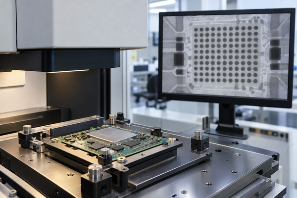
Inspect placement and solder joints with the agreed methods, including X‑ray when hidden joints beneath LGA, BGA, or other bottom‑terminated packages need examination. Record the specified electrical or functional results before release.
For repeat orders, PCB revision control, component‑lot identification, and controlled assembly settings help keep builds comparable. Review any change to components, PCB revision, soldering requirements, or test limits before the next production run.
How Are 5G Communication Module PCBs Tested?
Testing should follow the product state: a bare PCB needs electrical and impedance checks, a populated board needs assembly inspection, and a complete module or carrier may also need programmed functional and RF tests. These stages answer different questions and should not be treated as interchangeable.
| Test Stage | Method | Decision Provided |
|---|---|---|
| Bare PCB | Electrical test | Finds open circuits and unintended short circuits before assembly |
| Bare PCB | Impedance test coupons or approved test structures | Confirms specified transmission‑line impedance for the released stackup |
| SMT Process | Solder paste inspection (SPI) | Detects print‑volume or alignment problems before placement |
| Assembly | Automated optical inspection (AOI) | Checks visible placement, polarity, and soldering features |
| Assembly | X‑ray inspection | Examines hidden joints beneath LGA, BGA, and similar packages |
| Programmed PCBA | Functional test | Checks module startup, supply behavior, and specified interfaces using the provided procedure |
| Module or System | RF test | Measures only the agreed RF parameters with suitable fixtures, equipment, and limits |
Bare‑board electrical testing cannot prove 5G communication performance. RF output, antenna matching, network connectivity, and communication stability need separate module- or system‑level tests.
For assembled boards, provide the required firmware, test procedures, fixtures, and acceptance criteria before production. The factory can then confirm what it can test at board level and what remains the customer’s responsibility during final equipment integration.
What Affects 5G Communication Module PCB Lead Time?
Lead time is set by the longest constrained stage across PCB fabrication, material supply, component sourcing, assembly, and testing. A fast bare‑board build will not shorten the complete schedule if a specified module or RF connector is unavailable.
The main factors include:
- PCB Construction: HDI structures, microvias, via filling, and tight manufacturing tolerances can extend fabrication time.
- Material Availability: Low‑loss laminates and nonstandard materials may need additional sourcing or a customer‑approved alternative.
- Component Lead Time: Availability of 5G modules, RF connectors, and specified ICs affects assembly scheduling.
- Assembly Complexity: LGA packages, fine‑pitch components, shielding structures, and moisture‑sensitive parts may require extra preparation.
- Testing Requirements: Custom fixtures, firmware programming, functional tests, and report formats add engineering and production time.
For urgent projects, confirm component availability before committing to the PCB production schedule. Provide the required quantity, target delivery date, and shipping destination so manufacturing and transit time can be assessed separately.
EBest Circuit reviews expedited requests against the submitted manufacturing files, material requirements, component status, test scope, and available capacity. The confirmed schedule should reflect the complete deliverable, not only bare‑board fabrication.
Why Choose EBest Circuit for 5G Communication Module PCB Manufacturing?
EBest Circuit is a China‑based PCB and PCBA manufacturer that combines PCB fabrication, component sourcing, assembly, and inspection within one quotation path. Its verified product range includes multilayer and high‑frequency PCBs, while project‑specific HDI, material, impedance, and assembly requirements are reviewed against the submitted files.
- Custom PCB Manufacturing: Multilayer, HDI, high‑frequency, and hybrid PCB fabrication for applicable communication equipment projects.
- PCB and PCBA Services: PCB fabrication, component procurement, SMT assembly, through‑hole assembly, and agreed testing services.
- DFM Technical Support: Review of stackups, impedance specifications, fine‑pitch features, module footprints, and manufacturing tolerances before release.
- Prototype to Repeat Production: Prototype fabrication, small‑batch assembly, and repeat orders, with expedited options subject to material, component, and capacity review.
- Verified Quality Systems: The company lists ISO 9001:2015, ISO 13485:2016, IATF 16949, and AS9100D certifications. Buyers should confirm the applicable legal entity, site, certificate scope, and current revision during supplier qualification.
For projects involving LGA modules, RF connectors, controlled‑impedance traces, or specialized PCB materials, EBest Circuit can review fabrication and assembly requirements before quotation.
Contact sales@bestpcbs.com with your project specifications.
What Files Are Required for a 5G Communication Module PCB Quote?
A quote needs enough information to confirm PCB construction, component availability, assembly operations, test ownership, quantity, and schedule. Send the following available files; engineering review can identify any gaps before the scope is finalized.
- PCB Manufacturing Files: Gerber and drill files, fabrication drawing, and released stackup.
- Technical Specifications: Material, layer count, thickness, copper weight, surface finish, and impedance requirements.
- Component Information: BOM, selected 5G module part numbers, approved alternatives, and relevant datasheets.
- Assembly Files: Pick‑and‑place data, assembly drawings, polarity notes, module footprints, and special soldering instructions.
- Testing Requirements: Firmware, test procedures, fixtures, acceptance limits, and required records where applicable.
- Order Details: Prototype or production quantity, target delivery date, shipping destination, and any consigned material.
For LGA or M.2 projects, include the module datasheet, land pattern or connector specification, and mechanical drawing. Send the package to sales@bestpcbs.com for a manufacturing review and quotation.
FAQs About 5G Communication Module PCBs
Q1: Does every 5G module PCB require HDI technology?
A1: No. HDI is useful for dense routing and fine‑pitch packages, but a carrier board with less demanding routing may use conventional multilayer construction.
Q2: Can I supply my own 5G modem modules for assembly?
A2: Yes. Customer‑supplied modules can be accepted under agreed incoming‑inspection, storage, traceability, and assembly conditions.
Q3: Can different 5G modules share the same carrier PCB?
A3: Only when their footprints, pin assignments, power requirements, interfaces, mechanical constraints, and antenna connections are compatible. Confirm each point against the manufacturers’ datasheets.
Q4: Can RF shielding cans be installed during PCBA assembly?
A4: Yes, when the PCB includes the correct shielding footprint and assembly clearance. The shield and board design must also suit the specified soldering and rework processes.
Q5: Can firmware programming be included in production?
A5: Yes, when suitable programming interfaces, firmware files, instructions, fixtures, and acceptance criteria are available before assembly.
Q6: Does a 5G module PCB always require an integrated antenna?
A6: No. Some modules connect to external antennas through RF connectors or coaxial cables, while others use integrated or separate antenna structures.
Q7: Can several PCB revisions be manufactured for prototype evaluation?
A7: Yes. Each revision needs separately identified fabrication, assembly, BOM, and test files so the builds cannot be mixed.
Q8: Can 5G module PCBs be supplied in panels for automated assembly?
A8: Yes, if the panel design suits the board construction and assembly equipment. Review panel size, support rails, fiducials, tooling holes, and separation method before fabrication.
Q9: Can manufacturing files be shared under an NDA?
A9: Yes. Confidentiality arrangements can be discussed before sensitive designs, BOMs, or manufacturing documents are exchanged.
Q10: Does using a certified 5G module automatically certify the finished device?
A10: No. The completed product may still require regulatory evaluation based on its antennas, installation, operating configuration, enclosure, and intended market.
Conclusion
A 5G communication module PCB must match the electrical, mechanical, assembly, and test requirements of the selected module and host product. Confirm the material, stackup, impedance, footprint, thermal structures, component availability, and board‑level test plan before fabrication.
EBest Circuit provides custom PCB manufacturing and PCBA assembly for 5G module and carrier‑board projects. Send your Gerber files, stackup, BOM, module datasheet, assembly data, test requirements, quantity, and schedule to sales@bestpcbs.com for manufacturing review and quotation.
This entry was posted on Wednesday, October 14th, 2026 at 7:11 pm and is filed under pcb manufacturing.
You can follow any responses to this entry through the RSS 2.0 feed.
You can skip to the end and leave a response. Pinging is currently not allowed.
PakarPBN
A Private Blog Network (PBN) is a collection of websites that are controlled by a single individual or organization and used primarily to build backlinks to a “money site” in order to influence its ranking in search engines such as Google. The core idea behind a PBN is based on the importance of backlinks in Google’s ranking algorithm. Since Google views backlinks as signals of authority and trust, some website owners attempt to artificially create these signals through a controlled network of sites.
In a typical PBN setup, the owner acquires expired or aged domains that already have existing authority, backlinks, and history. These domains are rebuilt with new content and hosted separately, often using different IP addresses, hosting providers, themes, and ownership details to make them appear unrelated. Within the content published on these sites, links are strategically placed that point to the main website the owner wants to rank higher. By doing this, the owner attempts to pass link equity (also known as “link juice”) from the PBN sites to the target website.
The purpose of a PBN is to give the impression that the target website is naturally earning links from multiple independent sources. If done effectively, this can temporarily improve keyword rankings, increase organic visibility, and drive more traffic from search results.