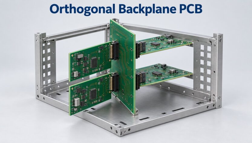
An orthogonal backplane PCB connects cards arranged at right angles, allowing high-speed signals to cross between them without long routes across a conventional backplane. This layout is used in networking and other modular electronic systems where board-to-board distance contributes to signal loss. Some designs retain a central PCB; direct orthogonal designs remove it from the high-speed connection.
EBest Circuit supports multilayer PCB fabrication, controlled-impedance construction, component sourcing and PCBA for customer designs. For an orthogonal backplane project, we can review the proposed board construction and assembly scope against your fabrication and connector requirements. Discuss your project with our team at sales@bestpcbs.com.
What Is an Orthogonal Backplane PCB?
An orthogonal backplane PCB is part of an interconnect structure in which one group of plug-in cards sits perpendicular to another. In a typical arrangement, vertical cards enter from the front of a chassis and horizontal cards enter from the rear. Their connectors meet at the crossing points.
In a network switch, the two card groups may perform different jobs:
- Line cards handle external network connections.
- Switch fabric cards carry traffic between line cards inside the system.
Placing these cards across one another allows each line card to connect to several switch fabric cards near their intersections. A conventional backplane instead carries signals along PCB traces between card connectors distributed across the board.
The word “orthogonal” describes the relative orientation of the cards. It does not specify a layer count, laminate or data rate. It also does not tell you whether the assembly contains a midplane PCB, which is the central board between the two card groups.
How Do Orthogonal Midplane and Direct Orthogonal Connections Differ?
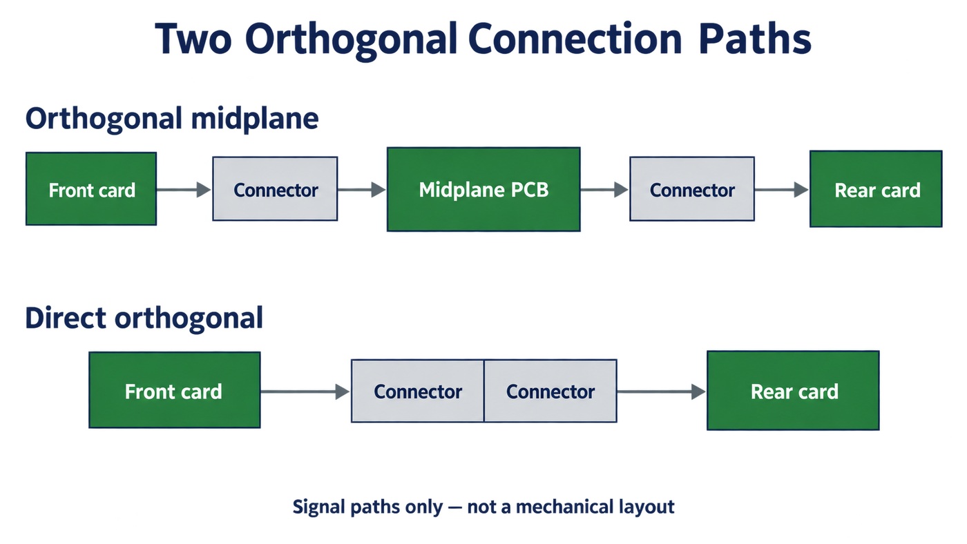
An orthogonal midplane retains a PCB between the cards. A direct orthogonal connection mates the perpendicular cards without that intermediate PCB in the high-speed path.
| Feature | Orthogonal midplane | Direct orthogonal |
|---|---|---|
| Central PCB | Remains between the card groups | Removed from the direct signal connection |
| Signal crossing | Passes through the midplane interconnect | Passes through the mating card connectors |
| Connector mounting | Opposing connectors attach to the midplane | Connectors attach to the intersecting cards |
| Mechanical reference | Midplane helps establish connector positions | Chassis guides and card supports establish alignment |
In one orthogonal midplane arrangement, connectors on opposite faces share signal and ground vias. The connection passes through the board instead of following a long lateral trace. Other power, management or inter-slot connections may still be routed within the midplane.
Direct orthogonal construction removes the intermediate board transition as well. However, it also removes the central mounting reference. Card guides, connector guidance features and the permitted movement between mating parts become more important because two separate cards must meet correctly inside the chassis.
“Backplane-free” therefore refers to the direct connection architecture. The system still contains PCBs and may use separate boards or cables for power and other functions.
How Does Orthogonal Backplane PCB Design Reduce Signal Loss?
Orthogonal backplane PCB design can reduce signal loss by shortening the distance a signal travels through PCB traces. A pass-through midplane replaces a long cross-board route with a short through-board connection. Direct orthogonal mating removes the intermediate PCB segment entirely.
The electrical benefit comes from the changed path:
- Less trace length: the signal encounters less conductor and dielectric loss along the removed route.
- A shorter central connection: a local pass-through avoids routing the same signal between distant backplane connectors.
- Fewer intermediate board transitions in a direct design: the channel no longer includes the removed midplane’s connector-to-PCB transitions.
Shorter does not mean lossless. The remaining connector contacts, PCB launches and vias still influence impedance, reflections and crosstalk. A launch is the transition between the connector and the board’s transmission line; poor geometry there can consume part of the benefit gained from a shorter route.
The relevant comparison is the complete channel from transmitter to receiver. Reducing its length can improve the loss budget, but the right-angle card arrangement alone cannot establish a maximum data rate or a fixed percentage improvement.
How Does an Orthogonal Card Layout Change Airflow?
An orthogonal card layout changes where boards and connectors obstruct air inside the chassis. It can open a more direct cooling path, particularly when a large central backplane is removed, but rotating the cards by 90 degrees does not automatically improve cooling.
With a midplane, air moving between the front and rear compartments must pass through available openings or around the board. Connector fields and routed areas limit where those openings can be placed.
With direct orthogonal mating, the central PCB no longer forms the same barrier. Space between connector groups may allow air to move through the card intersection more freely.
The remaining hardware still matters. Horizontal cards, heatsinks and support rails can block or redirect airflow even without a midplane. A useful cooling layout must carry air past the hot components on both card groups, rather than simply provide an open space in the middle of the enclosure.
What Materials and Layer Counts Do Orthogonal Backplane PCBs Use?
Orthogonal backplane PCBs do not have a standard material or layer count. The construction depends on whether the board carries long routed channels, short pass-through connections, or a mixture of signal and power functions.
| Board function | Main influence on construction |
|---|---|
| Routed high-speed channels | Dielectric loss, copper loss and controlled-impedance geometry |
| Short midplane pass-throughs | Connector footprint, plated-hole geometry and reference connections |
| Power and management routing | Current distribution, routing space and plane allocation |
For long high-speed routes, low-loss laminates can preserve more of the channel’s signal budget. A short pass-through structure may reduce that material burden, but its suitability still depends on the operating frequency and the complete connection. Neither standard FR-4 nor a premium low-loss laminate is the automatic answer for every orthogonal system.
Layer count follows the routing that remains. Signals need space to escape dense connector fields, while ground references and power distribution occupy additional layers. Removing lateral signal routes can reduce routing demand, although connector density and other board functions may still require a substantial multilayer stackup.
There is no universal 78-layer requirement. A layer count quoted for one high-density platform describes that particular design, not the definition of an orthogonal backplane PCB. Adding layers without a routing or electrical purpose also increases board thickness and manufacturing complexity.
How Does Orthogonal Backplane PCB Thickness Affect Vias and Connectors?
Orthogonal backplane PCB thickness affects both the distance signals travel through plated holes and the way connector pins engage those holes. A thicker board may provide useful stiffness, but its electrical and connector geometry must work together.
A through-board connection uses the via barrel.
When opposing connectors share a via through a midplane, the conductive barrel forms part of the intended signal path. That active section cannot be treated as unwanted copper simply because it passes through a thick board.
An unused via section is a different problem.
If a signal leaves a through-hole via on an inner layer, the barrel continuing beyond that connection can form a stub. At high frequencies, this unused branch can cause reflections and resonances. Backdrilling can remove the unwanted section where the design permits it, while retaining the required electrical connection and connector engagement.
Connector pins require a compatible board construction.
Press-fit contacts have defined compliant sections that engage plated holes. Board thickness, finished-hole size and the connector’s specified mounting geometry determine whether that engagement is correct. In a two-sided midplane, the opposing contacts and their insertion depths must also fit the intended shared-hole arrangement.
Board thickness is therefore tied to the selected interconnect. Increasing it for stiffness, or removing barrel copper for signal integrity, can change the same structure that holds and connects the pins.
How Are Connectors Mounted in Orthogonal Backplane PCB Assembly?
Connectors in orthogonal backplane PCB assembly may use press-fit or soldered termination, depending on the connector family. “Orthogonal” describes how the cards meet; it does not define how a connector attaches to its PCB.
Press-fit mounting
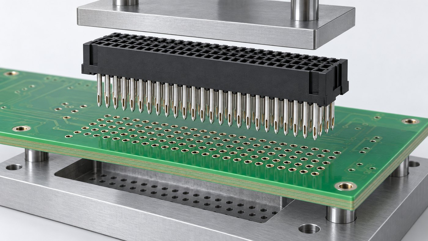
A compliant pin compresses as it enters a specified plated hole. The resulting contact provides electrical connection and mechanical retention without a solder joint at that interface.
For a dense connector array, the board is supported close to the insertion area and a suitable tool applies force through the connector’s intended pressing surfaces. This helps prevent board bending, bent pins and damage to the plated holes. Correct seating across the connector matters because an unevenly installed housing can misalign the mating interface.
Soldered mounting
Solder-terminated connectors require the assembly process specified for their mounting style. Surface-mount contacts use an appropriate reflow process; through-hole contacts use a suitable through-hole soldering process. Connector materials, board thermal mass and access to the joints influence the assembly method.
Card mating after assembly
Installing a connector on a PCB and plugging two cards together are separate operations. A connector can be securely attached to its board yet still meet the opposite card at the wrong position or angle. Chassis guides and connector alignment features help the mating contacts engage as intended without forcing the cards sideways.
Post-assembly inspection can identify seating and pin problems, while electrical testing can detect connection faults. Neither result alone demonstrates that the complete link meets its high-speed performance target.
FAQs About Orthogonal Backplane PCB
1. Is an orthogonal backplane PCB the same as orthogonal PCB routing?
No. An orthogonal backplane connects perpendicular cards. Orthogonal routing usually refers to traces running in different directions on adjacent PCB layers. The terms describe different levels of the design.
2. Are orthogonal backplanes used only in AI servers?
No. Orthogonal interconnects are also used in network switches, routers and other modular systems. Their relevance comes from the card arrangement and board-to-board connection distance, rather than an AI-specific function.
3. Is an orthogonal backplane always passive?
No. A midplane may provide passive interconnections, while another implementation may include power or management circuitry. Orthogonal card orientation does not determine whether active components are present.
4. Can a standard right-angle board-to-board connector replace an orthogonal connector?
Not automatically. A connector that turns a connection through 90 degrees may have a different mating geometry, pin assignment, electrical performance or alignment allowance. The angle alone does not make the connectors interchangeable.
5. Does passing a continuity test confirm high-speed signal performance?
No. Continuity testing checks electrical connections for faults such as opens and shorts. High-speed channel performance also depends on loss, impedance discontinuities and crosstalk, which require suitable analysis or measurements beyond a continuity test.
Planning an orthogonal backplane PCB or its mating card assemblies? Send your proposed stackup and connector details to sales@bestpcbs.com. EBest Circuit can discuss PCB fabrication and assembly options for your design, including impedance-controlled construction and the scope of production inspection and testing.
Tags: orthogonal backplane PCB, orthogonal backplane PCB assembly, orthogonal backplane PCB design
PakarPBN
A Private Blog Network (PBN) is a collection of websites that are controlled by a single individual or organization and used primarily to build backlinks to a “money site” in order to influence its ranking in search engines such as Google. The core idea behind a PBN is based on the importance of backlinks in Google’s ranking algorithm. Since Google views backlinks as signals of authority and trust, some website owners attempt to artificially create these signals through a controlled network of sites.
In a typical PBN setup, the owner acquires expired or aged domains that already have existing authority, backlinks, and history. These domains are rebuilt with new content and hosted separately, often using different IP addresses, hosting providers, themes, and ownership details to make them appear unrelated. Within the content published on these sites, links are strategically placed that point to the main website the owner wants to rank higher. By doing this, the owner attempts to pass link equity (also known as “link juice”) from the PBN sites to the target website.
The purpose of a PBN is to give the impression that the target website is naturally earning links from multiple independent sources. If done effectively, this can temporarily improve keyword rankings, increase organic visibility, and drive more traffic from search results.