
Electroless copper plating makes an insulating PCB hole wall conductive by depositing copper through a chemical reaction, without connecting the board to an external plating current. The thin deposit provides a base for subsequent copper electroplating. Reliable connections depend on continuous coverage of the resin, glass fibers and exposed inner-layer copper, not simply a copper-colored panel surface.
For a plated-through hole, the finished barrel must connect the intended copper layers and meet the specified final thickness. Chemical deposition starts that connection; electroplating builds most of its thickness. Confusing these two stages can leave a drawing with the wrong copper requirement or an inspection plan that checks the wrong feature.
What Is Electroless Copper Plating?
electroless copper plating is an autocatalytic metallization process. After suitable surface preparation and activation, dissolved copper ions are reduced to metallic copper on the treated surface. The deposited copper then supports continued deposition.
On a drilled FR4 PCB, the hole wall exposes insulating resin and glass as well as any intersected copper layers. Existing copper foil on the board faces cannot conduct electricity across those insulating surfaces. A continuous chemical copper layer creates the conductive foundation along the wall.
The term copper electroless plating describes the same deposition principle. It is not a synonym for the complete plated-through-hole process, a solderable final finish, or a mechanically inserted copper rivet. Those features have different functions and inspection requirements.
How Does Electroless Copper Plating Work?
A reducing agent supplies the electrons needed to convert copper ions into copper metal. A catalyst initiates deposition on the nonconductive material; no rectifier connection to the PCB is required during this chemical step.
An electroless copper plating solution contains a copper source, a reducing agent, complexing agents and process-control additives. The complexant keeps copper available in solution under the bath’s operating conditions. Stabilizers help limit unwanted deposition elsewhere in the tank. These functions must remain balanced as panels consume chemistry and solution ages.
Traditional systems often use formaldehyde as the reducing agent. Formaldehyde-free systems also exist, but changing the reducing chemistry changes the operating conditions and qualification requirements. A bath substitution is therefore a process change, not merely a label change.
In tartrate-based baths, Rochelle salt acts as a complexing agent. It is not the catalyst that initiates deposition on the dielectric, and it is not the deposited conductor. The applicable chemistry determines whether tartrate, EDTA or another complexant is used; they are not interchangeable additions to an existing bath.
What Are the Steps in the Electroless Copper Plating Process?
The electroless copper plating process prepares the drilled surfaces, activates the dielectric, deposits copper and preserves the deposit for the next operation. The detailed sequence depends on the laminate and chemistry, but the manufacturing tasks are consistent:
- Drill and remove debris. Establish the intended hole geometry without leaving loose material that can mask the wall.
- Desmear. Remove drilling resin smear, particularly where inner-layer copper must connect to the new hole barrel.
- Clean and condition. Prepare resin and glass for wetting and catalyst adsorption. Treat exposed copper as required by the selected process.
- Activate. Apply the catalyst system and complete its specified reduction or acceleration step where required.
- Deposit chemical copper. Maintain the qualified chemistry, temperature, immersion or conveyor time, and solution movement.
- Rinse and transfer. Prevent carryover, residue and damage before subsequent copper build-up.
A controlled electroless copper plating procedure also defines rinses between incompatible stages, bath-analysis frequency and the response to an out-of-control result. These are production controls rather than a universal mixing recipe. Adding more plating time cannot reliably compensate for an unactivated or contaminated area.
Why Are Desmear and Activation Important?
Desmear exposes the surfaces that must bond and connect; activation makes deposition start on the insulating wall. Failure in either stage can remain hidden beneath later copper.
Resin smear across an inner-layer edge can obstruct the intended copper-to-copper connection. Insufficient cleaning, poor conditioning or uneven catalyst adsorption can leave resin-rich or glass-rich areas incompletely covered. Aggressive treatment is not automatically better: the preparation must also preserve the laminate and hole geometry.
Microetching acts on exposed copper, while desmear removes resin residue. They are not substitutes for each other. For a deposit that looks satisfactory on the panel surface but fails inside holes, the investigation must include hole-wall preparation and wetting rather than only increasing copper concentration.
How Thick Should Electroless Copper Be on a PCB?
Electroless copper plating thickness must be sufficient for continuous coverage and the next manufacturing operation. The target is process-specific. A primary metallization seed layer should not be confused with the finished hole-wall copper specified on the fabrication drawing.
Low-build through-hole processes commonly use a thin seed deposit; semi-additive processes may require a different balance between coverage, conductivity and later seed-layer removal. A thicker surface deposit does not prove that the narrowest region of a microvia received adequate copper.
Specify the measurement location and stage. Surface copper, microvia-wall copper, via-bottom copper and final plated barrel thickness are different measurements. For a via-bottom-to-surface thickness ratio, the numerator must refer to the defined bottom location, not whichever point gives the largest result.
As an arithmetic example, 0.30 micrometers at the via bottom and 0.40 micrometers on the reference surface give a ratio of 75%. Those assumed numbers explain the calculation; they are not a production acceptance threshold. A deposit with an acceptable average can still contain a local skip.
Which Parameters Matter for PCB Hole Metallization?
The useful parameters connect the finished-board requirement to the geometry and deposition stages. Record units and measurement definitions before comparing results. The following dimensions distinguish our PCB fabrication capability limits from worked calculations and bath-specific controls.
| Parameter | Value, unit or calculation | How to use it |
|---|---|---|
| Layer count | Our FR4 capability: up to 32 layers, subject to engineering review | Identify each intended barrel-to-inner-layer connection in the stack-up. |
| Hole size | Our listed minimum hole size: 0.20 mm for conventional boards; 0.10 mm for HDI | Confirm whether the order specifies drilled or finished dimensions. HDI geometry needs its own build review. |
| Through-hole aspect ratio | Our listed maximum: 8:1; worked example: 1.60 mm board / 0.20 mm drilled hole = 8:1 | Use the actual drilled geometry for process assessment. This calculation is not an automatic approval of the example stack-up. |
| Average deposition rate | Thickness gain / deposition time; assumed example: 0.40 micrometers / 10 minutes = 0.040 micrometers/minute | Compare coupons at equivalent locations and conditions; average rate does not describe local coverage. |
| Bottom-to-surface ratio | Bottom thickness / surface thickness x 100%; assumed example: 0.30 / 0.40 x 100% = 75% | Record the sampling geometry and measurement method alongside the percentage. |
| Finished bore reduction | Approximately twice the radial deposit; assumed example: 25 micrometers per wall reduces diameter by about 50 micrometers | Apply to total deposited wall thickness, not only the chemical seed. Other processing and tolerances also affect the finished hole. |
| Bath temperature and pH | Record temperature in degrees C and pH against the specific chemistry control limits | No universal temperature or pH applies to all low-build, high-build and formaldehyde-free baths. |
| Copper/reducer concentration and bath age | Use the supplier’s specified analysis units and turnover or loading records | Track replenishment and contamination; do not infer bath condition from color alone. |
| Finished hole-wall copper | Drawing-specified minimum and, where applicable, average thickness in micrometers | Confirm the applicable product class, standard revision and inspection plan before manufacture. |
Our minimum feature sizes and maximum layer count are separate capability limits, not a promise that all extremes can be combined. Send the stack-up, drill file and final copper requirements together so we can evaluate the actual construction.
Electroless vs Electrolytic Copper Plating: What Is the Difference?
In electroless vs electrolytic copper plating, the central difference is how deposition is powered. Chemical deposition can establish conductivity on an activated dielectric; electrolytic deposition requires a conductive current path and typically supplies the subsequent copper build-up.
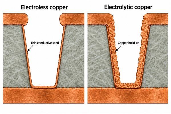
| Feature | Electroless copper | Electrolytic copper |
|---|---|---|
| Deposition driver | Chemical reduction at the activated surface | External electrical current |
| Starting surface | Properly prepared and activated dielectric or compatible conductive surface | Conductive surface with an adequate electrical connection |
| Typical PCB role | Primary metallization and conductive seed formation | Build-up of wall and surface copper; qualified processes may also fill vias |
| Key controls | Preparation, activation, bath chemistry, time, temperature and solution access | Current distribution, chemistry, agitation, time and electrical contact |
| Coverage concern | Skipped resin/glass areas or an incomplete connection interface | Uneven thickness, low local build or filling defects |
| What it cannot prove alone | Final hole-wall thickness or complete finished-board reliability | That an inadequately prepared underlying interface is sound |
These are usually complementary steps, not competing choices for the same operation. Direct metallization is another route to preparing a conductive hole wall; it does not eliminate the need to qualify the subsequent copper plating and finished interconnection.
What Causes Voids and Poor Copper Adhesion?
Voids can originate from incomplete preparation, activation or solution contact. Poor adhesion can involve the dielectric interface, residual contamination or deposit stress. The defect location and manufacturing stage help narrow the cause; appearance alone is not a root-cause analysis.
| Observed problem | Checks to prioritize | Useful distinction |
|---|---|---|
| Uncovered patches after chemical copper | Cleaning, conditioner/catalyst condition, rinsing, wetting and trapped air | A surface deposit elsewhere does not confirm coverage at the patch. |
| Defect near an inner-layer connection | Drilling residue, desmear effectiveness and the exposed copper interface | Separate a preparation/interface problem from low final barrel thickness. |
| Poor coverage at a blind-via bottom | Via geometry, debris, catalyst access and solution exchange | Compare bottom and wall locations instead of reporting surface thickness alone. |
| Blistering or separation | Surface contamination, material compatibility, preparation and deposit stress | Do not assume additional plating time restores adhesion. |
| Rough deposits or nodules | Bath stability, particulate contamination and filtration/control records | Distinguish deposit roughness from debris introduced during sample preparation. |
Keep the affected panel and its process history available while checking the relevant bath records. If a problem appears only after a thermal exposure, compare the interface and fracture location before assigning the fault to the chemical copper stage. Later electroplating, laminate behavior and hole geometry can also contribute.
How Is Electroless Copper Coverage Inspected?
Inspection combines evidence from the chemical copper stage with measurements after copper build-up. No single finished-board photograph can reconstruct all of the earlier process conditions.
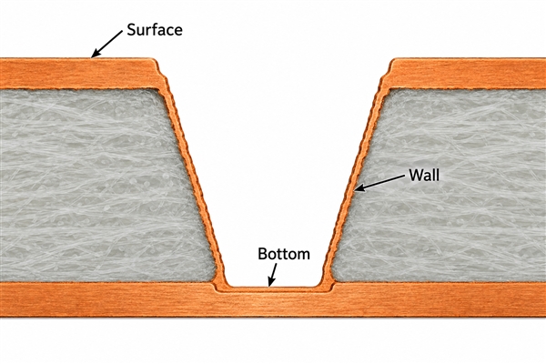
- Stage-specific coverage checks: examine representative coupons after primary metallization using the qualified method. Record where an uncovered region appears.
- Microsection analysis: inspect the hole wall and inner-layer connections at the sampled plane; measure the defined locations rather than one convenient point.
- Final copper measurements: evaluate the finished barrel requirement after the relevant plating stages.
- Electrical testing: check completed nets for opens and shorts. Passing continuity is not a measurement of adhesion or copper thickness.
- Specified reliability testing: assess the agreed thermal or interconnection requirements when they apply to the product.
Record the panel or coupon identification, inspected stage, hole type, section location, measurement results and disposition. A polished section samples a plane; it does not expose every point around every hole. Sample selection and escalation after a failed result are therefore part of the inspection plan.
How Does Horizontal Electroless Copper Plating Work?
Horizontal electroless copper plating transports panels through a horizontal processing line while chemistry contacts the surfaces and holes. The term describes equipment arrangement; the deposition is still chemical rather than powered by an external plating current.
Panel motion and controlled solution exchange help renew chemistry at the hole wall. In small or blind features, liquid access and gas removal deserve particular attention. Uniform transport does not, by itself, establish uniform local deposition.
Vertical systems can also produce qualified PCB metallization. Equipment choice must match panel handling, material, hole geometry and the qualified chemistry. Horizontal processing is not universally superior to vertical processing for every construction.
Conductive adhesive serves a different purpose. It creates a connection through an adhesive containing conductive material; it does not reproduce the continuous copper barrel formed by a metallization and plating sequence. The two cannot be exchanged in a PCB drawing without changing the interconnection design and its validation.
Which PCB Designs Need Electroless Copper Plating?
A common application of electroless copper plating is forming the initial conductor in plated holes and vias. Double-sided boards use it to connect the two copper faces; multilayer PCBs also require reliable connections to the intended inner-layer lands.
For HDI boards with blind microvias, the via bottom and the transition between wall and land require attention. A through-hole process setting cannot be assumed suitable for every laser-drilled feature or sequential-lamination structure.
Electroless copper plating on plastic and PCB metallization share the challenge of making a dielectric conductive, but decorative plastic plating is not the same manufacturing task. PCB laminates contain specific resin/glass systems and interlayer copper interfaces. On high Tg boards, the resin system must be compatible with the desmear, conditioning and metallization sequence; a higher glass-transition temperature alone does not establish that compatibility.
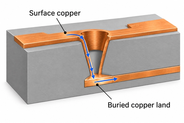
At EBest Circuit (Best Technology), we manufacture FR4 and HDI boards and provide DFM support for the complete PCB build. Our HDI options include blind and buried vias, laser drilling and sequential lamination. We review the hole structure, laminate, copper requirements and stack-up together to identify fabrication constraints before production.
What Affects Electroless Copper Plating Cost?
Electroless copper plating cost within a PCB order depends on geometry, material preparation, process loading and the required inspection. It is not determined by the weight of the thin copper deposit alone.
Small holes, greater depth, mixed dielectric systems and additional sequential build stages can change the processing and verification needed. Panel utilization and order quantity affect manufacturing efficiency, while special coupons, additional sections and agreed reliability tests add specific work.
For a board quotation, send us the Gerber or fabrication data, drill files, stack-up, laminate requirements, finished hole tolerances, copper requirements and quantities. Include any required inspection records or reliability conditions. Contact sales@bestpcbs.com so we can review the PCB construction and quote the relevant manufacturing scope.
Electroless Copper Plating FAQs
Does electroless copper plating need electricity?
It does not require an external plating current through the board. The production equipment may still use electricity for heating, pumping, conveying and control. The absence of a rectifier connection to the panel is the relevant distinction.
Is electroless nickel plating the same process?
No. Electroless nickel plating deposits a different metal or alloy system and commonly serves a different function. Nickel used in a final surface-finish stack does not replace the copper barrel that connects PCB layers.
Can chemical copper alone fill a PCB microvia?
A thin primary-metallization deposit coats a via; coating and filling are different outcomes. A filled-via requirement needs an explicitly qualified filling process and a defined acceptance requirement, not an assumption that a longer seed-deposition step will close the cavity correctly.
Why can a board pass continuity but still have a plating problem?
A conductive path can exist despite an undersized local copper section or a weak interface. Electrical testing identifies open and short circuits at the test conditions; thickness, adhesion and thermal durability need their corresponding evidence.
Tags: Electroless Copper Plating, PCB Metallization, plated through holes
PakarPBN
A Private Blog Network (PBN) is a collection of websites that are controlled by a single individual or organization and used primarily to build backlinks to a “money site” in order to influence its ranking in search engines such as Google. The core idea behind a PBN is based on the importance of backlinks in Google’s ranking algorithm. Since Google views backlinks as signals of authority and trust, some website owners attempt to artificially create these signals through a controlled network of sites.
In a typical PBN setup, the owner acquires expired or aged domains that already have existing authority, backlinks, and history. These domains are rebuilt with new content and hosted separately, often using different IP addresses, hosting providers, themes, and ownership details to make them appear unrelated. Within the content published on these sites, links are strategically placed that point to the main website the owner wants to rank higher. By doing this, the owner attempts to pass link equity (also known as “link juice”) from the PBN sites to the target website.
The purpose of a PBN is to give the impression that the target website is naturally earning links from multiple independent sources. If done effectively, this can temporarily improve keyword rankings, increase organic visibility, and drive more traffic from search results.