PCB teardrops are small copper reinforcements added where a trace connects to a pad, via, plated hole, or track junction. They reduce weak copper necks, improve drill tolerance, and help PCB fabrication stay more stable when the layout uses small pads, narrow traces, dense routing, or tight annular rings.
In real manufacturing, slight drill shift, etching variation, layer registration tolerance, and thermal stress can affect copper continuity. PCB teardrops give critical transition points more copper support without changing the circuit function. When used correctly, they improve DFM quality, reduce avoidable production defects, and support more reliable PCB assembly.
What Are PCB Teardrops in PCB Design?
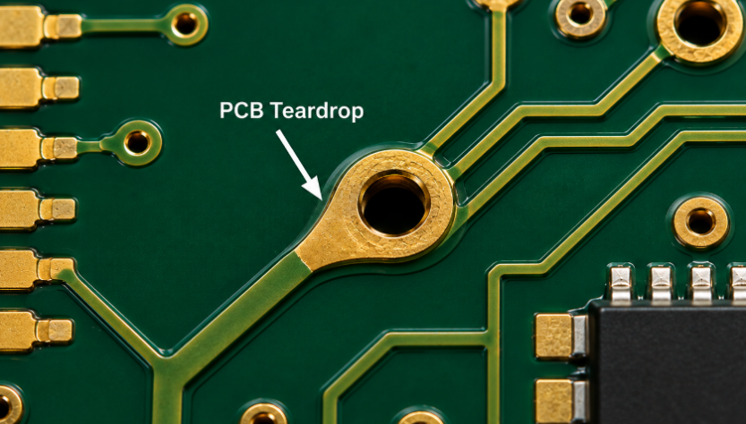
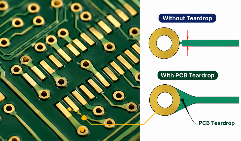
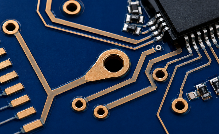
PCB teardrops are tapered copper extensions placed between a PCB trace and a pad, via, plated through hole, or track junction. The copper gradually widens from the narrow trace into the larger copper feature, creating a stronger and smoother transition.
The working principle is simple: a teardrop in PCB design increases the copper area at the weakest connection point. If drilling is slightly off-center or etching removes a small amount of copper, the reinforced area still has more margin than a plain narrow neck.
PCB teardrops are a DFM improvement, not a repair method for poor layout rules. Correct pad size, annular ring, drill tolerance, trace width, spacing, and solder mask clearance must still be designed properly before teardrops are added.
What Does a Teardrop Look Like on a PCB?
A teardrop PCB feature usually looks like a small drop-shaped, oval, rounded, or tapered copper area where a trace enters a pad or via. It is wider near the pad and narrower near the trace, so the copper transition does not look abrupt.
On a via, it may look like a smooth copper neck flowing into a round via pad. On an SMD pad, it may look like a short copper wedge connected to the pad edge. On a track junction, it may appear as a rounded fillet that softens the width change.
A good teardrop should be clean, centered, and controlled. It should not touch another net, create copper slivers, break clearance rules, or interfere with solder mask openings. The final shape must be checked in the real copper output, not only in the layout view.
What Types of Teardrops Are Commonly Used in PCB Layout?
Common teardrops in PCB layout include curved arc teardrops and straight linear teardrops. The right type depends on board density, signal speed, reliability level, available spacing, and manufacturing tolerance.
- Curved Arc Teardrops
Curved arc teardrops use a rounded copper transition from the trace to the pad, via, or track junction. The smooth edge helps distribute mechanical stress more evenly and provides better geometry continuity. This type is recommended for high-frequency PCB, high-reliability PCB, automotive electronics, medical PCB, aerospace PCB, and Class 3 reliability designs. - Straight Linear Teardrops
Straight linear teardrops use a diamond-like or linear copper transition. They occupy less routing space and are easier to fit into compact PCB layouts. This type is suitable for ordinary low-speed PCB, dense HDI routing, 0201 components, fine-pitch QFN pads, and tight fanout areas.
For high-reliability or high-speed PCB design, curved arc teardrops are usually preferred. For compact low-speed layouts where spacing is limited, straight linear teardrops can be a more practical choice.
Why Use Teardrops on PCB Pads, Vias and Tracks?
Teardrops are used because pads, vias, and track junctions are common weak points in PCB copper geometry. A narrow trace entering a larger pad may lose copper margin if drilling, imaging, or etching has normal production variation.
- Pads: Teardrops reinforce SMD pads, through-hole pads, connector pads, and component lands. This helps reduce trace neck damage near solder joints and improves reliability under thermal cycling or mechanical force.
- Vias: Teardrops reduce drill breakout risk around small via pads and tight annular rings. They are useful in dense routing, HDI PCB, BGA fanout, and multilayer PCB designs where registration tolerance is limited.
- Tracks: Teardrops smooth trace width changes, T-junctions, and neck-down areas. This reduces sharp copper stress points and helps avoid open circuits caused by weak copper transitions.
For customers, the practical value is fewer open circuits, lower rework risk, more stable prototype validation, and better batch production yield.
How Do PCB Teardrops Improve PCB Manufacturing Quality?
PCB teardrops improve manufacturing quality by adding copper margin at points affected by drilling, imaging, plating, etching, and layer registration tolerances. These tolerances are normal in PCB fabrication, especially on dense multilayer boards and small via designs.
During drilling, the hole may not land exactly in the center of the pad. During etching, a narrow trace may lose a small amount of copper width. If the trace-to-pad neck is already weak, the remaining copper can become too thin or even open. PCB teardrops reduce this risk by widening the transition area.
They also support better process stability when the board has small annular rings, fine traces, fine-pitch pads, and compact via fanout. In batch production, this can reduce scrap, lower inspection pressure, and improve long-term reliability.
For PCBA projects, teardrops also help protect copper near pads that experience soldering heat, connector insertion force, vibration, or repeated thermal cycling. They do not replace good fabrication control, but they add useful manufacturing tolerance.
When Should PCB Teardrops Be Used?
PCB teardrops should be used when the layout has limited copper margin, small pads, narrow traces, tight drilling tolerance, or high reliability requirements. They are most valuable when a normal manufacturing shift could weaken a copper connection.
Use teardrops in these cases:
- Small vias with tight annular rings or limited pad diameter.
- Fine traces connected to larger pads, vias, or plated holes.
- Through-hole connectors exposed to plug-in force or vibration.
- Flex and rigid-flex PCB near bend exits or rigid-to-flex transitions.
- High-vibration electronics used in automotive, industrial, robotics, or outdoor equipment.
- Dense multilayer PCB where layer registration tolerance is tighter.
- Prototype designs moving into stable batch production.
If pads are large, traces are wide, spacing is generous, and reliability demand is low, teardrops may not bring obvious manufacturing value. In that case, clean routing and standard DFM rules are more important.
Where Are Teardrops Commonly Used in PCB Layout?
Teardrops are commonly used at trace exits, via connections, plated hole pads, connector pads, fine-pitch component pads, and narrow track junctions. These areas often carry higher manufacturing, assembly, or mechanical risk.
Typical locations include:
- Via fanout areas near ICs, BGAs, and dense routing channels.
- Connector pads where repeated insertion may stress solder joints.
- Through-hole pads for terminals, headers, switches, and power pins.
- Fine-pitch SMD pads where trace width is much smaller than pad width.
- Flex PCB pad exits where copper fatigue may happen.
- Track neck-down areas where trace width changes sharply.
- High-current transition areas where copper continuity matters.
- Test pads and programming pads that may face repeated probing.
The best location is not every pad or every via. It is the area where added copper improves reliability without creating clearance, solderability, impedance, or inspection problems.
What PCB Teardrop Size Rules and Design Specifications Should Be Followed?
PCB teardrop size rules should follow PCB manufacturer capability, copper spacing, annular ring, solder mask clearance, drill tolerance, and signal requirements. There is no single universal size for every teardrop PCB design.
A practical rule is to make the teardrop large enough to reinforce the copper neck, but small enough to avoid spacing and mask issues. Small vias and large vias should not use the same setting. HDI routing usually needs smaller, cleaner teardrops because clearance is more limited.
For SMD pads, the teardrop should not disturb solder mask openings or solder paste behavior. For high-speed nets, the shape should not create a large sudden copper widening. For rigid-flex PCB, rounded shapes are usually safer than sharp transitions.
| Item | Typical Range | Checkpoint |
|---|---|---|
| Via length | 25%–50% pad diameter | Drill margin |
| Via width | 50%–80% pad diameter | Annular support |
| SMD length | 75%–150% trace width | Pad transition |
| SMD width | 150%–250% trace width | Mask spacing |
| Track length | 100%–300% trace width | Copper neck |
| Clearance | Supplier DFM rule | Net safety |
| Shape | Rounded or straight | Layout density |
Before production, confirm PCB teardrop size rules with the PCB manufacturer, especially for HDI PCB, impedance-controlled PCB, RF PCB, rigid-flex PCB, and fine-pitch assembly. If a teardrop causes spacing violations, solder mask conflict, or impedance concern, reduce the size or remove it from that area.
How Do Teardrops Affect High-Speed PCB Design?
Teardrops can affect high-speed PCB design because they add local copper area and slightly change trace-to-pad geometry. In many standard digital or low-speed circuits, the effect is small. In controlled impedance, RF, and high-speed differential routing, it should be reviewed carefully.
Use extra care in these areas:
- Controlled impedance traces where copper widening may change local impedance.
- Differential pairs where both sides should keep similar shape, width, and length.
- RF launch areas where pad geometry is part of the tuned transition.
- High-speed via fanout where return path, anti-pad, and via stub all matter.
- BGA escape routing where clearance and symmetry are limited.
- Clock, DDR, PCIe, USB, Ethernet, and antenna paths where geometry consistency matters.
High-speed designs can still use teardrops, but they should be selective and symmetrical. Avoid large automatic teardrops on RF launch pads, impedance-controlled neck-downs, or matched differential pairs unless the final geometry has been reviewed.
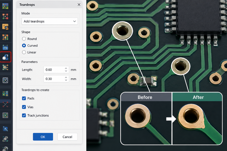
How to Add Teardrops in KiCad?
KiCad teardrops should be added after the main routing is complete and before final manufacturing output. This avoids repeated changes when traces, vias, pads, or copper zones are still being adjusted.
Step 1: Finish the main PCB routing.
Complete trace routing first, including via placement, pad connections, copper pours, differential pairs, and key spacing rules. Do not add teardrops too early, because later routing changes may distort the teardrop shape or create clearance issues.
Step 2: Check basic design rules.
Run DRC before adding teardrops. Fix trace width, via size, pad clearance, annular ring, and net spacing problems first. PCB teardrops should reinforce a correct layout, not cover existing rule violations.
Step 3: Set teardrop parameters.
Open the teardrop settings and define the shape, length, width, and target objects. For round vias and through-hole pads, use moderate teardrops to improve drill tolerance. For rectangular SMD pads, keep the shape smaller to avoid solder mask or pad spacing problems.
Step 4: Apply teardrops to selected areas.
Apply teardrops to vias, pads, or track junctions based on real need. Small vias, narrow traces, fine-pitch pads, flex PCB exits, and connector pads should be prioritized. Avoid applying large teardrops automatically across high-speed or RF areas.
Step 5: Refill copper zones and run DRC again.
After adding teardrops, refill all copper zones and run DRC again. Check whether any teardrop creates clearance errors, copper slivers, solder mask conflicts, or unwanted copper connections.
Step 6: Review final output files.
Inspect the final Gerber, ODB++, or IPC-2581 files before sending them to the PCB manufacturer. Make sure the PCB teardrops are visible on the correct copper layers and do not affect impedance-sensitive nets, fine-pitch pads, or assembly areas.
How to Use Teardrops in Altium Designer?
Altium Designer teardrops should also be used near the final stage of PCB layout, after routing, rule setup, and major copper changes are stable. This keeps the teardrop geometry clean and easier to verify before PCB fabrication.
Step 1: Complete routing and confirm design rules.
Finish all critical routing first, including differential pairs, impedance traces, vias, polygon pours, and connector fanout. Then confirm trace width, clearance, via size, solder mask, and manufacturing rules.
Step 2: Open the teardrop tool.
Use the teardrop command in the PCB editor to add, modify, or remove teardrops. Select whether the teardrops should apply to pads, vias, tracks, or T-junctions. For dense boards, it is better to apply them by selected object type or selected area.
Step 3: Choose the teardrop style.
Use curved arc teardrops for high-reliability, high-frequency, automotive, medical, aerospace, and Class 3 PCB designs. Use straight linear teardrops for ordinary low-speed boards, compact HDI layouts, 0201 components, and fine-pitch QFN areas where spacing is limited.
Step 4: Control size and clearance.
Set the length and width according to pad size, trace width, and available spacing. Do not make teardrops too large. Oversized copper may reduce clearance, affect solder mask openings, or change local impedance around high-speed nets.
Step 5: Apply teardrops and inspect sensitive areas.
After applying teardrops, manually check fine-pitch SMD pads, via fanout areas, differential pairs, RF traces, connector pads, and polygon connections. Remove or reduce any teardrop that creates spacing risk or unwanted copper geometry.
Step 6: Run DRC and review manufacturing data.
Run DRC after teardrops are added. Then review the final copper output to confirm that all teardrops are clean, connected to the correct nets, and suitable for PCB manufacturing. For batch production, ask the PCB supplier to include teardrop geometry in the DFM review.
What Mistakes Should Be Avoided When Using PCB Teardrops?
The biggest mistake is adding PCB teardrops automatically without reviewing the final copper geometry. Teardrops should improve manufacturability, not create new production or signal risks.
Avoid these mistakes:
- Using oversized teardrops that violate copper clearance or create solder mask conflict.
- Adding teardrops to every object without considering real manufacturing need.
- Ignoring fine-pitch SMD pads where extra copper may affect solderability.
- Creating asymmetry on differential pairs, RF paths, and matched routes.
- Using teardrops to hide poor annular ring design instead of fixing pad and drill rules.
- Forgetting to refill polygon pours after teardrop generation.
- Skipping Gerber or ODB++ output review before fabrication release.
- Allowing duplicate teardrops from both CAD layout and CAM engineering.
- Ignoring supplier DFM feedback when teardrops create clearance or plating risk.
A good teardrop should be clean, useful, and manufacturable. If it makes inspection harder, reduces spacing, changes a tuned high-speed transition, or conflicts with assembly requirements, it should be reduced or removed.
FAQs About PCB Teardrops
Q1: Can teardrops reduce open-circuit failures in PCB fabrication?
A1: Yes. PCB teardrops can reduce open-circuit risk by adding extra copper at weak trace-to-pad and trace-to-via junctions. This is useful when the trace is narrow or the annular ring is tight. For boards with fine lines below 4 mil, small vias, or dense fanout, teardrops can provide more tolerance against etching loss and drill shift.
Q2: Do teardrops help if the drill hole is slightly off-center?
A2: Yes, but only within reasonable manufacturing tolerance. A teardrop gives the via or plated hole more copper support near the trace connection, so minor drill offset is less likely to break the copper neck. However, it cannot fix a poorly designed annular ring. The pad and drill design should still meet the supplier’s standard tolerance, such as ±3 mil or project-specific capability.
Q3: Are teardrops suitable for HDI PCB routing?
A3: Teardrops can be useful in HDI PCB routing, but the size must be controlled carefully. HDI designs often use microvias, fine traces, and compact BGA fanout, so large teardrops may violate spacing rules. For HDI boards, smaller curved or linear teardrops are usually safer. Clearance, solder mask, via pad size, and final CAM output should be reviewed before production.
Q4: Can teardrops be used on blind vias and buried vias?
A4: Yes. Teardrops can be used on blind vias and buried vias when the CAD tool and PCB manufacturer support the design. They are helpful when the via pad is small or the trace connection is narrow. For HDI stackups, the teardrop geometry should match the via structure, lamination process, and layer registration tolerance. Always confirm with the factory before batch production.
Q5: Will teardrops affect solder paste printing?
A5: They may affect solder paste printing if the teardrop extends too close to the exposed SMD pad area. This is more critical for 0201 components, fine-pitch QFN, BGA pads, and connector pads. The copper shape should not change the paste opening or create solder bridging risk. Solder mask and stencil design should be checked together with the teardrop layout.
Q6: Should teardrops be added to test points?
A6: Teardrops can be added to test points when the pad is small, the trace is narrow, or the point may experience repeated probe contact. They can improve copper strength around the pad edge. For ICT or functional test pads, keep enough spacing around the pad and avoid shapes that may affect probe contact accuracy, especially when test pads are below 1.0 mm.
Q7: Are teardrops useful for connector reliability?
A7: Yes. Connector pads often face insertion force, vibration, cable movement, and thermal cycling. Teardrops can strengthen the copper transition between the trace and the connector pad. This is useful for headers, terminals, board-to-board connectors, and wire harness connectors. For high-stress connectors, teardrops should be combined with proper pad size, mechanical support, and solder joint design.
Q8: Can teardrops help rigid-flex PCB durability?
A8: Yes. Rigid-flex PCB designs often benefit from smooth copper transitions near pad exits and rigid-to-flex transition areas. Rounded teardrops can reduce stress concentration and improve copper fatigue resistance. For dynamic bending applications, avoid vias, sharp corners, and abrupt copper width changes in the bend area. Bend radius, copper grain direction, and coverlay opening should also be reviewed.
Q9: Do teardrops improve current carrying capacity?
A9: Not significantly. Teardrops add copper at a local transition, but they do not replace proper current-carrying design. Current capacity mainly depends on copper thickness, trace width, temperature rise, layer structure, and thermal dissipation. For high-current PCB designs, teardrops may help strengthen transitions, but wider traces, copper pours, thermal vias, and heavier copper are more important.
Q10: Can teardrops be removed after they are generated?
A10: Yes. Most PCB design tools allow teardrops to be modified or removed. They should be removed if they create clearance violations, solder mask conflicts, copper slivers, impedance concerns, or unwanted asymmetry on matched signals. Before fabrication, the final Gerber, ODB++, or IPC-2581 data should be reviewed to confirm that all remaining teardrops are clean and manufacturable.
Q11: Are teardrops better than increasing pad size?
A11: They solve different problems. Increasing pad size improves annular ring and drill tolerance, while teardrops reinforce the trace connection area. If space allows, correct pad sizing is usually the first solution. Teardrops are most helpful when the pad size is limited by dense routing, fine-pitch components, or HDI layout constraints. They should support good design, not replace it.
Q12: What should be confirmed with the PCB manufacturer before using teardrops?
A12: Confirm the manufacturer’s copper spacing, drill tolerance, annular ring capability, solder mask clearance, minimum trace width, and CAM modification policy. For critical projects, also confirm whether the factory will add or adjust teardrops during CAM engineering. For batch orders, request a DFM review before production, especially for HDI PCB, RF PCB, rigid-flex PCB, and Class 3 PCB.
Q13: Do teardrops matter more in prototype or mass production?
A13: They matter in both stages, but the value is different. In prototype builds, teardrops help reduce avoidable fabrication risk and support faster design validation. In mass production, they help stabilize yield and reduce repeated defects. For products moving from prototype to batch production, teardrops should be reviewed together with DFM, assembly process, and inspection criteria.
Q14: Can automatic teardrop generation create hidden problems?
A14: Yes. Automatic generation may create oversized shapes, spacing conflicts, copper slivers, or asymmetry on high-speed nets. This is why DRC and CAM review are necessary after adding teardrops. Automatic tools are useful, but final judgment should consider board density, solder mask, impedance control, via type, and assembly requirements. Critical areas should always be checked manually.
Q15: What is the best file format for teardrop review?
A15: Gerber files are widely accepted, but ODB++ and IPC-2581 are often better for intelligent manufacturing review because they include structured layer and net information. For a complete review, send copper layers, drill files, solder mask, paste layers, stackup, fabrication notes, and netlist. This helps the manufacturer verify teardrop geometry before fabrication and PCBA assembly.
Conclusion
PCB teardrops help improve copper reliability at pads, vias, and track junctions. They are especially useful for fine traces, small vias, HDI PCB, rigid-flex PCB, connector areas, and high-reliability products.
Use teardrops selectively, not blindly. Before production, review annular ring, drill tolerance, solder mask clearance, impedance control, Gerber output, and assembly requirements together. EBest Circuit provides custom PCB fabrication, PCB layout review, DFM checking, PCBA assembly, and global supply. Send your Gerber, ODB++, stackup, BOM, and assembly files for review and quotation: sales@bestpcbs.com.
Tags: pcb teardrop size rules, teardrop in pcb, teardrops in pcb layout, teardrops pcb design
PakarPBN
A Private Blog Network (PBN) is a collection of websites that are controlled by a single individual or organization and used primarily to build backlinks to a “money site” in order to influence its ranking in search engines such as Google. The core idea behind a PBN is based on the importance of backlinks in Google’s ranking algorithm. Since Google views backlinks as signals of authority and trust, some website owners attempt to artificially create these signals through a controlled network of sites.
In a typical PBN setup, the owner acquires expired or aged domains that already have existing authority, backlinks, and history. These domains are rebuilt with new content and hosted separately, often using different IP addresses, hosting providers, themes, and ownership details to make them appear unrelated. Within the content published on these sites, links are strategically placed that point to the main website the owner wants to rank higher. By doing this, the owner attempts to pass link equity (also known as “link juice”) from the PBN sites to the target website.
The purpose of a PBN is to give the impression that the target website is naturally earning links from multiple independent sources. If done effectively, this can temporarily improve keyword rankings, increase organic visibility, and drive more traffic from search results.