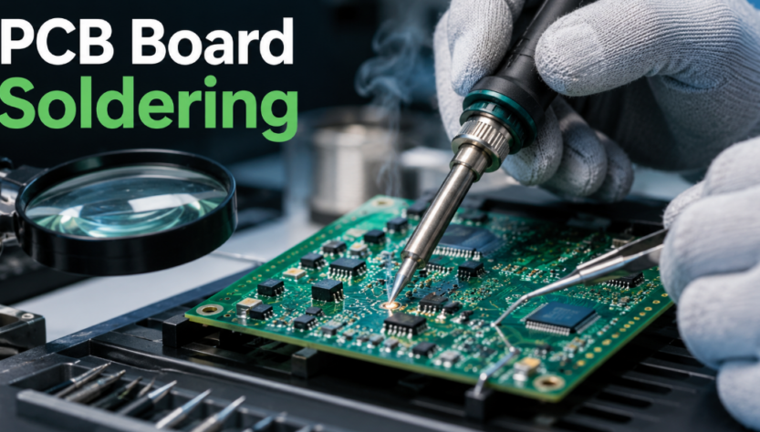
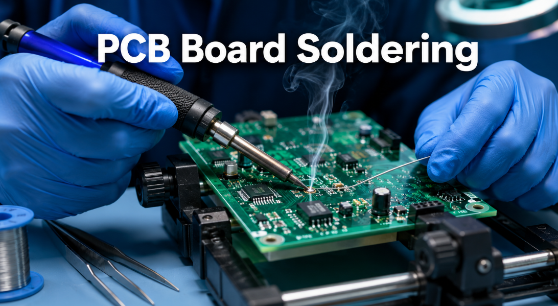
PCB board soldering joins electronic components, wires, connectors and terminals to a printed circuit board through controlled heat and molten solder. A good solder joint provides stable conductivity, mechanical strength and long-term reliability, while a poor joint may cause intermittent signals, short circuits, overheating or early product failure.
This guide explains soldering in PCB board assembly from a practical production view. It covers tools, soldering iron selection, temperature, solder wire, solder paste, holders, cleaning, solderability, defects, testing, cost and supplier selection. It is written for prototype work, repair projects, OEM assembly, ODM production and batch PCBA manufacturing.
What Is PCB Board Soldering?
PCB board soldering is the process of bonding component leads, pads, wires or terminals to a PCB with molten solder. The solder forms a conductive metal connection after it wets the pad and cools into a stable joint.
This process is used for through-hole parts, surface mount devices, connectors, switches, sensors, cables and prototype circuits. A good joint should look smooth, fully wetted and mechanically secure.
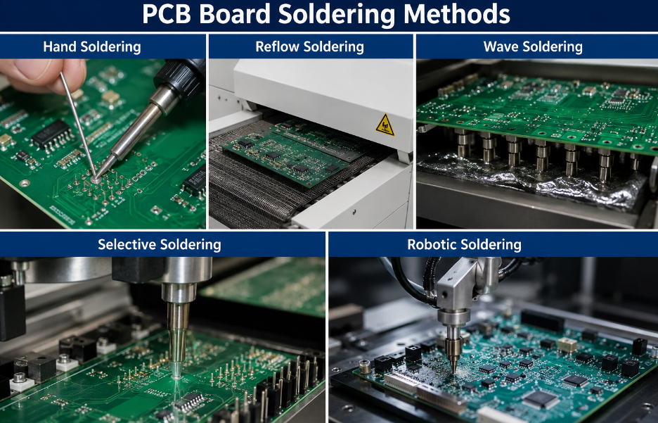
In production, PCB board soldering can be done by hand soldering, reflow soldering, wave soldering, selective soldering or robotic soldering. The best method depends on component type, volume, reliability level and inspection requirements.
Why Does PCB Board Soldering Matter for Assembly Reliability?
PCB board soldering matters because most circuit problems appear at connection points before they appear in the circuit design itself. A weak solder joint can pass an early power test but fail later under vibration, heat, humidity or repeated use.
For industrial control boards, IoT devices, medical equipment, automotive modules and communication products, soldering quality affects signal stability, current carrying capacity and product life. Even a small solder bridge can damage a board.
Reliable soldering also reduces repair cost after shipment. When the soldering temperature, flux, solder wire, solder paste and inspection process are controlled, the finished PCBA is easier to approve and more stable in real applications.
How Does Soldering in PCB Board Assembly Work?
Soldering in PCB board assembly works through heat transfer, wetting and solidification. The soldering iron or machine must heat both the PCB pad and the component lead before solder can flow correctly.
First, the pad and lead must be clean enough for solder to wet the surface. Then heat is applied to the joint area instead of only touching the solder wire. Once the metal surfaces reach the right temperature, solder flows around the lead and pad.
After that, the heat source is removed, and the joint cools without movement. If the component moves during cooling, the joint may become cracked, dull or weak. This same principle applies to hand soldering, reflow soldering and selective soldering.
What Tools Are Used for PCB Board Soldering?
PCB board soldering tools depend on whether the job is repair, prototype assembly or mass production. A basic PCB board soldering kit usually includes a soldering iron, soldering wire, flux, tweezers, tip cleaner, solder wick and a PCB board holder for soldering.
For hand work, a temperature-controlled PCB board soldering iron is better than a low-cost fixed-temperature tool. It gives more stable heat and reduces cold joints, pad damage and poor wetting.
For factory assembly, a PCB board soldering machine may include a reflow oven, wave soldering system, selective soldering machine, solder paste printer or robotic soldering system. These machines improve consistency for batch PCBA production.
| Tool | Use Case | Application |
|---|---|---|
| Soldering Iron | Manual joints | Repair, wire soldering, prototypes |
| Hot Air Station | SMD rework | ICs, resistors, capacitors |
| PCB Holder | Board support | Stable hand soldering |
| Soldering Stand | Iron safety | Tip protection and work safety |
| Reflow Oven | SMT assembly | Batch PCBA production |
| Wave Soldering | Through-hole parts | Connectors and DIP components |
| Selective Soldering | Local soldering | Mixed assembly projects |
| AOI System | Inspection | SMT solder quality check |
How to Choose the Best Soldering Iron for PCB Boards?
The best soldering iron for PCB boards should have stable temperature control, fast heat recovery, replaceable tips and comfortable handling. For most PCB work, a 40W to 80W temperature-controlled soldering station is more useful than a cheap high-heat iron without control.
For fine SMD parts, use a smaller tip with good thermal response. For connectors, ground pads and thick copper boards, use a larger tip that can transfer enough heat without staying on the pad too long.
When choosing a soldering iron for PCB board repair or prototype work, also check tip availability, ESD safety, handle comfort and temperature accuracy. A good iron reduces rework risk and makes soldering pcb boards easier to repeat.
Useful selection points include:
- Choose temperature control for stable hand soldering.
- Match tip size to pad size and copper area.
- Use ESD-safe tools for sensitive components.
- Select fast heat recovery for large pads and connectors.
- Keep spare tips for fine pitch, through-hole and wire soldering.
- Avoid holding the iron on the pad for too long.
What PCB Board Soldering Temperature Should Be Used?
PCB board soldering temperature depends on solder alloy, pad size, copper thickness, board finish and component heat sensitivity. For hand soldering, lead-free solder often works around 330–380°C, while leaded solder often works around 300–350°C.
Higher temperature is not always better. Excessive heat may burn flux, damage components, lift pads or discolor the laminate. Low temperature may melt solder slowly but fail to heat the pad enough, which causes cold joints.
For large copper areas or power connectors, a wider tip may solve the problem better than raising temperature. The best setting is the lowest temperature that still creates fast, smooth and complete solder wetting.
| Solder Type | Range | Note |
|---|---|---|
| Leaded Sn63/Pb37 | 300–350°C | Fast wetting and lower heat demand |
| Lead-Free SAC305 | 330–380°C | Higher melting point and more heat demand |
| Fine SMD Pads | 300–360°C | Short contact time protects parts |
| Large Ground Pads | 350–400°C | Larger tip improves heat transfer |
| Wire to PCB Pad | 330–380°C | Pre-tinning improves joint quality |
What Materials Affect PCB Printed Circuit Board Assembly Solderability?
PCB printed circuit board assembly solderability is affected by solder alloy, flux, surface finish, pad design, copper thickness, component plating and storage condition. Even skilled soldering cannot fully solve oxidation, poor plating or expired solder paste.
PCB board soldering wire is mainly used for manual work, wire soldering, through-hole assembly and repair. PCB board soldering paste is used for SMT production, where paste is printed on pads before placement and reflow.
Surface finish also changes soldering behavior. HASL, ENIG, OSP, immersion silver and immersion tin have different wetting performance and storage sensitivity. For batch production, incoming inspection and proper material storage reduce solderability risks.
| Material | Effect | Risk |
|---|---|---|
| Solder Wire | Manual joint formation | Weak wetting or excess solder |
| Solder Paste | SMT solder volume | Voids, bridges or insufficient solder |
| Flux | Oxide removal | Residue, corrosion or poor wetting |
| Surface Finish | Pad solderability | Dewetting or non-wetting |
| Copper Thickness | Heat absorption | Slow solder flow |
| Component Plating | Joint bonding | Unstable contact |
| PCB Storage | Oxidation control | Difficult soldering |
What Are the Main PCB Board Soldering Methods?
The main PCB board soldering methods are hand soldering, reflow soldering, wave soldering, selective soldering and robotic soldering. Each method has a different role in prototype work, SMT production, through-hole assembly and mixed technology PCBA manufacturing.
Hand soldering is flexible for repair, wires and PCB prototype board soldering. Reflow soldering is used for most SMT components because it supports speed and repeatability. Wave soldering is efficient for boards with many through-hole leads.
Selective soldering is useful when through-hole parts must be soldered after SMT reflow without heating the entire board. Robotic soldering works well for repeated wire, terminal and connector joints when fixtures are stable.
Main functions include:
- Hand soldering supports repair, sample changes and small batches.
- Reflow soldering supports high-volume SMT assembly.
- Wave soldering handles many through-hole joints efficiently.
- Selective soldering protects nearby sensitive components.
- Robotic soldering improves repeatability for fixed joint positions.
Main limitations include:
- Hand soldering depends strongly on operator skill.
- Reflow soldering requires correct paste, stencil and profile control.
- Wave soldering may create bridges if layout and process settings are poor.
- Selective soldering is slower than wave soldering for dense boards.
- Robotic soldering requires repeatable board positioning and fixtures.
How to Solder a PCB Board Step by Step?
How to solder a PCB board starts with preparation, correct heating and clean inspection. The key rule is to heat the pad and lead together, then feed solder into the heated joint instead of melting solder directly on the iron tip.
First, secure the PCB in a PCB board holder for soldering so the board does not move. Clean the pad, prepare the component, set the proper temperature and tin the soldering iron tip. A clean, lightly tinned tip transfers heat faster.
Next, touch the tip to both the pad and component lead. Feed solder wire into the joint area until it flows around the metal surfaces. Remove the solder first, then remove the iron. Let the joint cool naturally before moving the board.
Finally, inspect the joint under good lighting or magnification. A good joint should show complete wetting, stable shape and no bridge to nearby pads. Clean residue if the flux type or product environment requires cleaning.
How to Solder Wire to PCB Board Safely?
Soldering wire to PCB board requires strain relief, correct wire preparation and controlled heat. A wire joint should not rely on solder alone to carry mechanical pulling force, especially in products exposed to vibration or repeated handling.
First, strip only the required wire length and twist the strands neatly. Pre-tin the wire and the PCB pad so the final soldering time is shorter. Then place the wire on the pad and heat both surfaces until the solder flows together.
For production, use cable ties, adhesive, slots, terminals or mechanical fixtures when the wire may be pulled. This protects the copper pad from lifting. After soldering, inspect for broken strands, excess solder, insulation damage and weak fillet shape.
Key control points include:
- Pre-tin the wire and PCB pad before final joining.
- Avoid too much exposed conductor outside the joint.
- Add strain relief when the wire may move.
- Keep insulation away from direct iron contact.
- Avoid pulling the wire before the joint cools.
- Use inspection to confirm full wetting and no loose strands.
How to Clean PCB Board After Soldering?
Cleaning a PCB board after soldering depends on flux type, product environment and reliability level. No-clean flux may remain on many standard products, but high-reliability, high-impedance, RF, medical or harsh-environment boards often require cleaner residue control.
First, identify the flux chemistry. Rosin, water-soluble and no-clean fluxes require different cleaning methods. Using the wrong cleaner can spread residue or leave ionic contamination on the board.
For manual cleaning, use approved electronic-grade cleaner, lint-free swabs and controlled brushing. Avoid soaking sensitive parts unless the process is approved. After cleaning, dry the board fully before power testing because trapped moisture may cause leakage current or corrosion.
In batch production, cleaning should be part of the process plan. The supplier should control cleaning materials, drying time, inspection criteria and contamination risk before shipment.
What Common PCB Board Soldering Defects Should Be Avoided?
Common PCB board soldering defects include cold joints, solder bridges, insufficient solder, excess solder, lifted pads, poor wetting, tombstoning, solder balls, voids and cracked joints. Most defects come from poor heat transfer, wrong solder volume, contamination or unstable process control.
Cold joints may look dull, rough or cracked, and they often cause intermittent electrical failure. Solder bridges create shorts between nearby pads or pins. Insufficient solder reduces mechanical strength and current reliability.
Lifted pads often come from overheating, repeated rework or pulling parts before the solder fully melts. Flux residue may also become a risk when it is conductive, corrosive or trapped under components.
| Defect | Cause | Prevention |
|---|---|---|
| Cold Joint | Low heat or movement | Heat pad and lead together |
| Solder Bridge | Excess solder | Control solder volume |
| Lifted Pad | Overheating or force | Use short contact time |
| Poor Wetting | Oxidation or contamination | Clean pad and use flux |
| Solder Ball | Paste or flux issue | Control paste and profile |
| Tombstoning | Uneven heating | Balance pad design and reflow |
| Voids | Outgassing or paste issue | Optimize paste and profile |
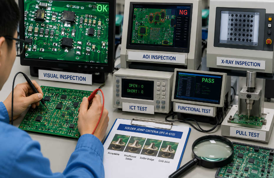
How Is PCB Board Soldering Tested and Inspected?
PCB board soldering is tested by visual inspection, AOI, X-ray, ICT, flying probe, functional testing, pull testing and reliability testing. The right inspection method depends on component package, board complexity, product risk and solder joint visibility.
Visual inspection works for through-hole joints, wires and simple repairs. AOI is common for SMT production because it checks missing parts, polarity, bridges and solder shape. X-ray is used for hidden joints such as BGA, QFN and LGA packages.
Electrical tests confirm that joints are not only visually acceptable but also functional. For high-reliability products, thermal cycling, vibration testing, humidity testing and aging tests help reveal weak joints before shipment.
| Test | Detects | Use |
|---|---|---|
| Visual | Obvious solder defects | Wires and through-hole joints |
| AOI | SMT placement and solder issues | Production inspection |
| X-ray | Hidden solder joints | BGA, QFN and LGA |
| ICT | Open and short circuits | Batch PCBA testing |
| Flying Probe | Prototype electrical faults | Low-volume boards |
| FCT | Product operation | Finished assemblies |
| Pull Test | Mechanical joint strength | Wire and terminal soldering |
What Quality Standards Apply to PCB Board Soldering?
PCB board soldering quality is commonly controlled by IPC workmanship standards, RoHS material compliance, customer drawings and factory process controls. IPC-A-610 is widely used for electronic assembly acceptability, while IPC J-STD-001 focuses on soldering process requirements.
RoHS compliance is important for lead-free electronic products sold in many global markets. Some projects may also involve ISO quality systems, UL material requirements, automotive reliability control, medical traceability or customer-specific inspection rules.
Standards are only useful when the factory applies them in daily production. A reliable manufacturer should control solder paste storage, stencil printing, reflow profile, soldering temperature, operator training, inspection records and corrective actions.
| Standard | Focus | Use |
|---|---|---|
| IPC-A-610 | Acceptability | Visual assembly criteria |
| IPC J-STD-001 | Soldering process | Workmanship and process control |
| RoHS | Substance control | Lead-free compliance |
| ISO 9001 | Quality system | Process management |
| UL | Safety materials | Product compliance support |
| Customer Spec | Project rules | Custom inspection criteria |
What Factors Affect PCB Board Soldering Cost?
PCB board soldering cost is affected by component count, package type, soldering method, testing level, order volume, manual labor and reliability requirements. Fine-pitch SMT, BGA, mixed assembly, wire soldering and strict inspection usually increase total assembly cost.
For prototype orders, setup time may be a large part of the price. For mass production, cost depends more on process stability, yield, testing speed and rework rate. Poor files or unclear soldering notes can also increase communication and rework cost.
The best cost control method is early file review. Gerber files, BOM, pick-and-place file, assembly drawing, soldering notes, test plan and packaging rules help the factory quote accurately and avoid delays.
| Factor | Impact | Control |
|---|---|---|
| Component Count | More assembly time | Optimize BOM |
| Fine Pitch | Higher inspection demand | Use proper stencil |
| BGA/QFN | X-ray may be required | Confirm early |
| Wire Soldering | More labor | Add drawings and fixtures |
| Mixed Assembly | More process steps | Plan sequence |
| Testing Level | Higher quality cost | Match risk level |
| Quantity | Setup cost changes | Use pilot run |
How to Choose a Reliable PCB Board Soldering Manufacturer?
Choose a PCB board soldering manufacturer by checking process capability, inspection systems, solderability control, engineering review and batch production experience. A reliable China source factory should support OEM manufacturing, ODM production, sample development, custom assembly and global delivery without claiming false overseas locations.
For international buyers, the lowest quote is not always the safest choice. A good supplier reviews soldering risks before production, confirms process routes and gives practical feedback on pads, wires, connectors, heat-sensitive parts and inspection needs.
Supplier selection points include:
- Confirm SMT, through-hole, selective soldering and manual soldering capability.
- Check whether the factory supports PCB prototype board soldering and mass production.
- Ask about solder paste storage, reflow profiling and soldering temperature control.
- Confirm AOI, X-ray, ICT, FCT and visual inspection options.
- Review IPC workmanship understanding and RoHS compliance support.
- Choose clear communication, real factory capability and stable delivery over the lowest price.
FAQs About PCB Board Soldering
Q1: Is it okay to put soldering iron on PCB board?
A1: It is okay to touch the soldering iron tip to the PCB pad during soldering, but it should not stay there too long. Long contact time may lift pads, burn flux or damage laminate. Heat the pad and lead quickly, feed solder, then remove the iron.
Q2: What is the best soldering iron for PCB boards?
A2: The best soldering iron for PCB boards is usually a temperature-controlled ESD-safe soldering station with replaceable tips. For most repair and prototype work, 40W to 80W is practical. Stable heat recovery and correct tip size matter more than maximum wattage.
Q3: What is a PCB board holder for soldering used for?
A3: A PCB board holder for soldering keeps the board steady while both hands work on the soldering iron and solder wire. It reduces movement during cooling, which helps prevent cracked joints, cold joints and accidental bridges during manual soldering.
Q4: What soldering wire should be used for PCB board work?
A4: PCB board soldering wire should match product compliance and solderability requirements. Lead-free SAC solder is common for RoHS products, while leaded solder is easier for some repair work. Flux-core wire is often used for manual soldering because it improves wetting.
Q5: Why does soldering on PCB board sometimes look dull?
A5: A dull joint may be normal for some lead-free solders, but a rough, grainy or cracked surface can indicate a cold joint. Check heat transfer, flux activity, pad cleanliness and movement during cooling before accepting the joint.
Q6: What is the difference between PCB board soldering paste and soldering wire?
A6: PCB board soldering paste is used for SMT assembly and reflow soldering, while soldering wire is used for hand soldering, repair, wires and through-hole joints. Paste requires stencil printing and controlled storage, while wire is fed directly into the heated joint.
Q7: How to soldering PCB board without damaging pads?
A7: The correct phrase is “how to solder a PCB board,” and the safest method is to use controlled temperature, proper tip size, enough flux and short contact time. Avoid pulling components before solder fully melts because force can lift copper pads.
Q8: Why does solder not stick to a PCB board?
A8: Solder may not stick because the pad is oxidized, dirty, too cold or poorly plated. Clean the pad, apply suitable flux and heat the pad and lead together. If the surface finish is damaged, the board may have a solderability problem.
Q9: Can soldering PCB boards be done without flux?
A9: Some solder wire contains flux core, so extra flux may not always be required. However, additional flux often improves wetting and reduces rework, especially on old pads, wires, connectors or difficult surfaces. The flux type should match cleaning requirements.
Q10: What is PCB prototype board soldering used for?
A10: PCB prototype board soldering is used to verify circuits, test components, modify samples and prepare small pilot builds. It is more flexible than mass production, but final batch assembly still requires process review, solderability control and inspection planning.
Q11: How to clean PCB board after soldering if flux remains?
A11: Use an approved electronics cleaner, lint-free swabs and controlled brushing based on the flux type. Water-soluble, rosin and no-clean fluxes require different cleaning decisions. After cleaning, the board should be fully dry before power testing.
Q12: What causes solder bridges on PCB soldering board projects?
A12: Solder bridges are usually caused by excess solder, fine pad spacing, poor stencil design, too much paste or unstable hand soldering. Better solder volume control, proper flux, AOI inspection and pad design review can reduce bridge risk.
Q13: What files are required for PCB board soldering quotation?
A13: For quotation, provide Gerber files, BOM, pick-and-place file, assembly drawing, soldering notes, test requirements and order quantity. If the board has wires, connectors or hand-soldered parts, add photos or detailed drawings to reduce misunderstanding.
Q14: Can a China PCB factory handle global PCB board soldering orders?
A14: Yes. A real China source factory can support OEM, ODM, sample development and batch PCB assembly for global customers. The key is transparent capability, clear documentation, controlled quality and honest global delivery support, not false overseas factory claims.
Conclusion
PCB board soldering is a core assembly process that directly affects electrical stability, mechanical strength and long-term product reliability. Good soldering depends on correct heat transfer, clean materials, suitable solder wire or paste, controlled soldering temperature, stable fixtures, proper inspection and clear production standards. For prototypes, hand soldering offers flexibility. For mass production, SMT reflow, wave soldering, selective soldering, AOI, X-ray and functional testing provide stronger consistency.
When selecting tools, choose a stable soldering iron, proper tip size, suitable solder wire, clean flux and a reliable PCB board holder for soldering. When selecting a supplier, focus on solderability review, process capability, inspection records, communication quality and real factory experience. A capable manufacturer can support PCB prototype board soldering, custom PCBA assembly, OEM production, ODM development and batch manufacturing with better cost control and fewer quality risks.
If you are looking for reliable OEM manufacturing, ODM production, sample development, mass production, or custom engineering solutions, please contact our engineering team for technical support and a quote: sales@bestpcbs.com.
Tags: best soldering iron for pcb boards, pcb board holder soldering, pcb board soldering iron, soldering iron for pcb board
PakarPBN
A Private Blog Network (PBN) is a collection of websites that are controlled by a single individual or organization and used primarily to build backlinks to a “money site” in order to influence its ranking in search engines such as Google. The core idea behind a PBN is based on the importance of backlinks in Google’s ranking algorithm. Since Google views backlinks as signals of authority and trust, some website owners attempt to artificially create these signals through a controlled network of sites.
In a typical PBN setup, the owner acquires expired or aged domains that already have existing authority, backlinks, and history. These domains are rebuilt with new content and hosted separately, often using different IP addresses, hosting providers, themes, and ownership details to make them appear unrelated. Within the content published on these sites, links are strategically placed that point to the main website the owner wants to rank higher. By doing this, the owner attempts to pass link equity (also known as “link juice”) from the PBN sites to the target website.
The purpose of a PBN is to give the impression that the target website is naturally earning links from multiple independent sources. If done effectively, this can temporarily improve keyword rankings, increase organic visibility, and drive more traffic from search results.