
Stray capacitance is an unintended electric-field connection between conductors. On a PCB, it can form from a pad or trace to a plane, between adjacent traces, across a component footprint, through a connector, or inside the measurement setup. Its value may be tiny, yet its impedance falls as frequency rises. That makes the same geometry harmless in one circuit and decisive in another.
Understanding the number requires more than a definition. The useful path is to locate the coupling geometry, make a first-order estimate, connect the capacitance to a circuit symptom, separate the fixture from the board during measurement, and turn the result into a specific layout action.
What Is Stray Capacitance?
Any two conductors separated by an insulator create capacitance because an electric field can store charge between them. A schematic shows intended capacitors, but the physical assembly adds many more. These unintended contributions are called stray capacitance or parasitic capacitance. They are distributed throughout packages, traces, pads, planes, cables, fixtures, and nearby metal rather than concentrated in one named component.
It is unavoidable because real conductors always have area, separation, and a dielectric environment. Whether it matters depends on the conductors it connects, the frequency content of the signal, and the impedance of the affected node. The first task is to identify the unintended electric-field path rather than assume every small capacitance is harmful.
What Causes PCB Stray Capacitance?
Start by drawing the two conductors that form the unintended capacitor and the dielectric between them. This prevents vague instructions such as “add more spacing” when the dominant path may actually be vertical overlap to a plane or a package pin.
| Coupling pair | What increases it | Typical concern | Review action |
|---|---|---|---|
| Trace to plane | Long/wide copper, thin dielectric, higher Dk | Added load or return-path coupling | Check overlap, reference choice, and layer spacing |
| Trace to trace | Small gap and long parallel run | Crosstalk between aggressor and victim | Increase spacing or reduce parallel exposure |
| Pad/via to plane | Large pad, small antipad, plane proximity | Load at sensitive nodes | Review padstack and plane clearances |
| Across a footprint | Close pads, long stubs, copper underneath | Oscillator, feedback, or sensor error | Use vendor layout and control local copper |
| Board to chassis/cable | Large facing area and close metal | Common-mode current and EMC behavior | Model the physical assembly, not only the PCB |
What Is the Stray Capacitance Formula?
The general definition is C = Q/V. For two broad conductors facing each other, the first-order geometry formula is C ≈ ε₀εᵣA/d. It shows that capacitance rises with conductor overlap and dielectric permittivity, then falls as the conductors move farther apart. This relationship explains why larger pads, thinner dielectrics, and longer overlapping runs usually add capacitance.
The formula is an approximation for PCB structures. Coplanar traces, fringing fields, solder mask, vias, packages, plane cutouts, and nearby metal distort the field. Use it to understand direction and approximate scale. Use a two-dimensional or three-dimensional field solver when the exact value affects impedance, stability, timing, sensing accuracy, or an isolation-current limit.
How Do You Calculate Stray Capacitance?
Begin with the conductor pair that creates the unwanted electric field. Choose a model that matches its geometry, calculate a range rather than one perfect value, and then place that range into the circuit. A capacitance estimate becomes useful only after it is connected to frequency, node impedance, and an acceptable performance limit.
- Define the conductor pair: name the aggressor and victim or the node and reference metal.
- Select the geometry model: plate, coplanar trace, via, package, cable, or a full 3D structure.
- Use the real stackup: include dielectric thickness and the material property’s applicable test condition.
- Sweep tolerances: test spacing, dielectric and registration ranges rather than one nominal number.
- Insert the result into the circuit: verify its effect across frequency and operating conditions.
A Worked First-Order PCB Example
Assume a 20 mm section of 0.25 mm-wide copper overlaps a reference plane across a 0.20 mm dielectric. For an initial estimate, use a relative permittivity of 4.0. The overlapping area is 20 mm × 0.25 mm = 5 mm², or 5 × 10⁻⁶ m². The separation is 0.20 mm, or 2 × 10⁻⁴ m.
C ≈ ε₀εᵣA/d = (8.854 × 10⁻¹²)(4.0)(5 × 10⁻⁶)/(2 × 10-4) ≈ 0.89 pF. At 1 MHz, that capacitance has about 179 kΩ of reactance. At 100 MHz, it has about 1.79 kΩ. The geometry has not changed, but its ability to carry AC current has changed by a factor of 100.
This is not a finished PCB model. The calculation assumes uniform parallel fields and ignores trace-edge fringing, solder mask, local resin content, copper thickness, nearby conductors, cutouts, packages, and frequency-dependent material behavior. Use it to decide whether the effect is plausibly negligible or worth extracting. If 0.5 pF versus 1.2 pF would change the circuit decision, sweep that range in the circuit simulation and obtain a field-solver or measured value before release.
How Does Stray Capacitance Affect a Circuit?
The same parasitic element can create different symptoms depending on where it connects. At a high-impedance input it can reduce bandwidth or increase settling time. Between an amplifier output and input it can alter feedback and phase margin. Between adjacent signals it can inject crosstalk. Across an isolation barrier it can carry common-mode current during fast voltage transitions.
Analog Devices documents an example in which 1 pF of added capacitance at a high-speed amplifier’s inverting input produced almost 2 dB of frequency-response peaking. That number belongs to the documented circuit, not every amplifier. Its broader lesson is that a value that appears negligible on a BOM can be significant when the node is sensitive and the bandwidth is high.
- Bandwidth loss: capacitance combines with source or feedback resistance to create an unintended pole.
- Instability or ringing: an added pole or resonant path reduces margin.
- Crosstalk: displacement current from a fast aggressor appears on a nearby victim.
- Timing and frequency error: unintended load changes RC timing or oscillator conditions.
- Measurement offset: the fixture, cable, probe, and empty board add capacitance to the reported result.
Use the Symptom to Find the Coupling Path
| Observed symptom | Likely capacitive path | Discriminating check | Action if confirmed |
|---|---|---|---|
| Peaking, ringing, or oscillation | Output or nearby fast node coupling into an amplifier input or feedback node | Add the estimated capacitance to the loop model, then compare bandwidth and transient response with a layout variant | Reduce sensitive-node copper and overlap while preserving the intended return path |
| A quiet trace moves when an adjacent net switches | Long parallel trace exposure or connector-pin coupling | Correlate victim amplitude with aggressor edge rate and temporary spacing or shielding changes | Reduce parallel length, increase separation, reroute, or control the aggressor edge |
| Unexpected common-mode current or emissions | Switch node to chassis, cable, shield, or isolated secondary | Measure current versus dV/dt and compare enclosure or cable configurations | Reduce facing area or control the return path without defeating safety spacing |
| Capacitance changes when the setup moves | Probe, cable, fixture, hand, or nearby metal coupling | Fix the geometry, repeat OPEN correction, and compare an empty-board baseline | Use a rigid fixture, shorter connections, shielding, and repeatable calibration planes |
What Happens to Stray Capacitance at High Frequency?
A capacitor’s reactance is XC = 1/(2πfC). Increasing frequency lowers the opposition that a capacitive path presents. A small parasitic that looks almost open at low frequency can therefore shunt a high-frequency signal, feed an output back into an input, or couple a fast edge into a quiet node.
Edge rate matters as much as clock frequency. A digital net that switches only occasionally can still contain substantial high-frequency energy when its rise and fall times are short. Review the bandwidth of the transition and the impedance of the victim node instead of deciding from the repetition rate alone. The same edge-rate, return-path, via, and crosstalk relationships are covered in more detail in our high-speed digital PCB design guide.
- High-impedance nodes: even a small displacement current can create a meaningful voltage error.
- Wide-band amplifiers: added feedback or load capacitance can reduce phase margin and produce peaking or oscillation.
- Fast-switching power nodes: capacitive current can cross isolation or reference boundaries and contribute to common-mode noise.
- Timing networks: extra capacitance changes charge time, oscillator load, delay, or measurement settling.
How Do You Measure Stray Capacitance?
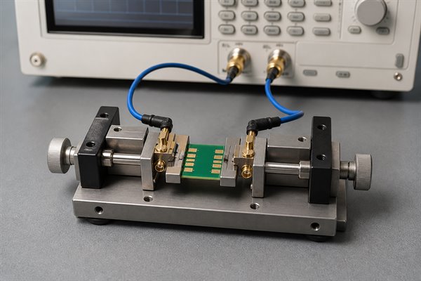
Measurement must separate the device under test from the test system. Leads, clips, probes, cables, fixtures, hands, and the empty PCB can all contribute. TDK notes that an open fixture still adds capacitance, while Murata explains that a change in fixture-terminal geometry between OPEN correction and measurement changes the residual error.
Use an OPEN correction with the same fixture position and spacing as the real measurement. Keep cables and nearby objects fixed. For an assembled sensitive node, compare a baseline structure without the component with the populated result when the method permits it. Analog Devices uses this approach in an op-amp input-capacitance measurement: it first determines the board/test stray term without the amplifier, then includes the device.
- Stabilize the setup: fix cable routing, fixture spacing, shielding and environmental conditions.
- Measure the baseline: perform OPEN correction or characterize the empty footprint/board structure.
- Use the relevant frequency: capacitance meters and impedance analyzers can report different behavior as frequency changes.
- Repeat after movement: a changed fixture or cable position invalidates a delicate baseline.
- Correlate with circuit behavior: confirm that the extracted value explains the observed pole, frequency shift, crosstalk or current.
Choose the Measurement Method by the Decision You Need
| Method | Best use | What it actually returns | Main limitation |
|---|---|---|---|
| Geometry calculation | Early screening and sensitivity sweeps | A first-order estimate for a defined conductor pair | Weak for irregular, coplanar, package, connector, or enclosure fields |
| 2D or 3D field extraction | Stackup, trace, via, connector, and enclosure structures | A capacitance matrix or geometry-specific model | Only as accurate as the geometry and material inputs |
| LCR meter or impedance analyzer | Accessible nodes, coupons, fixtures, and low-capacitance structures | Total impedance interpreted through the selected equivalent-circuit model | Fixture, cable, parallel paths, test level, and frequency can dominate |
| Empty-board or unpopulated-footprint baseline | Separating board and fixture contribution from a component result | A difference between two closely controlled configurations | Board variation and re-fixturing error can be comparable to the value being extracted |
| TDR | Locating and modeling a discontinuity in a transmission structure | A time-positioned impedance disturbance from which excess capacitance may be derived | It does not replace an LCR measurement for every lumped low-frequency node |
OPEN correction removes parallel stray admittance only when the open configuration represents the same calibration plane and fixture geometry used for the DUT. SHORT correction addresses series residual impedance. Murata’s fixture study shows why terminal spacing during OPEN correction must match the measurement geometry; Keysight likewise treats fixture compensation as part of the measurement rather than an optional cleanup step. Record frequency, signal level, equivalent-circuit mode, cable position, fixture dimensions, compensation state, temperature when relevant, and repeatability across several connections.
How Can You Reduce Stray Capacitance on a PCB?
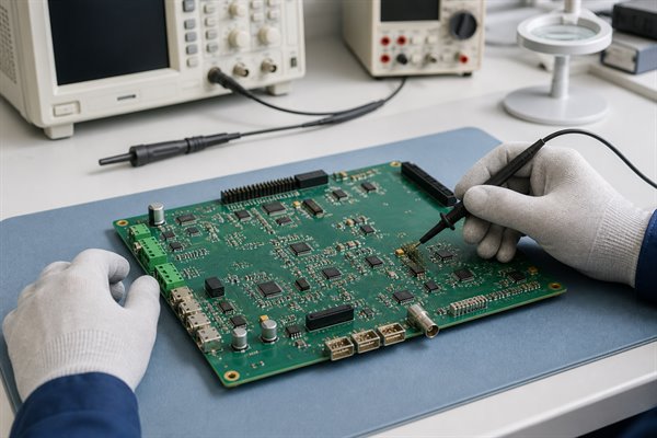
Reduce the electric-field coupling that matters, not copper indiscriminately. Changing one geometry can improve capacitance while harming return paths, impedance, shielding, thermal spreading, EMC, or manufacturability. The right action follows from the conductor pair and circuit symptom already identified.
| Layout or circuit action | Why it can work | Tradeoff to check | Verification |
|---|---|---|---|
| Reduce overlap or parallel run length | Less shared electric field reduces mutual or trace-to-plane capacitance | A longer detour may add loop area, inductance, delay, or new coupling | Re-extract the complete route and compare timing, crosstalk, and return continuity |
| Increase spacing between aggressor and victim | Field strength and mutual capacitance generally fall with separation | Board area, escape routing, differential geometry, and manufacturing rules | Sweep spacing with the actual stackup and check the victim-noise limit |
| Remove plane copper under a sensitive pad or node | It removes one plate of the dominant local capacitor | Return-path discontinuity, EMI, impedance change, thermal spreading, and plane necking | Review return-current flow and simulate both the local node and neighboring transmission structures |
| Use a grounded shield or driven guard | It intercepts or follows the electric field before it reaches the victim | A grounded shield can increase load to ground; a driven guard needs a stable low-impedance driver | Measure leakage, stability, bandwidth, and residual coupling over the intended frequency range |
| Increase dielectric separation or use lower Dk | The plate estimate predicts lower capacitance | Controlled impedance, board thickness, material availability, loss, and cost | Recalculate the complete stackup and obtain fabricator confirmation before release |
| Lower victim impedance or slow the aggressor edge | The same coupled current creates less voltage, or lower dV/dt creates less displacement current | Driver loading, power, timing margin, settling, and functional bandwidth | Simulate worst-case source/load corners and confirm on the prototype |
A reduction is complete only when it passes the original circuit limit. Define that limit before changing the layout: allowable victim voltage, phase-margin target, settling error, frequency shift, common-mode current, or fixture uncertainty. Compare the original and revised geometry under the same assumptions, sweep fabrication tolerances, and repeat the same prototype test. Keep the stackup revision, extraction setup, instrument correction state, and result with the design record so a later board spin does not recreate the same coupling path.
What Is the Difference Between Stray Inductance and Stray Capacitance?
Stray capacitance stores energy in an electric field between conductors, while stray inductance stores energy in the magnetic field around a current path. Capacitance is strongly affected by conductor overlap, separation, dielectric material, and the voltage transition between nodes. Inductance is strongly affected by current-loop area, conductor length, return-path continuity, and package or via geometry.
Both can exist in the same PCB structure and resonate together. A fast switch node can couple current through capacitance while its commutation loop adds inductance; the combination can produce ringing. Reducing one parasitic without checking the other can move the resonant frequency rather than solve the problem. Model the complete current and electric-field path before changing planes, spacing, vias, or loop geometry.
FAQs About Stray Capacitance
Q1: Is stray capacitance the same as parasitic capacitance?
A1: The terms are often used interchangeably for unintended capacitance. “Parasitic” can also describe a modeled non-ideal element inside a component, package, trace, or via. The useful question is which two conductors form the capacitance and how that path affects the circuit.
Q2: Can stray capacitance be eliminated completely?
A2: No. Any separated conductors create an electric field and therefore capacitance. The practical goal is to reduce or control the dominant coupling paths until the circuit meets its margin. Some applications intentionally use controlled capacitance, so eliminating all coupling would not even be desirable.
Q3: Does a wider PCB trace increase stray capacitance?
A3: It can increase trace-to-plane capacitance because the overlapping area grows. The actual result also depends on length, dielectric thickness, nearby copper, solder mask, and field fringing. Do not narrow a power, impedance-controlled, or thermal trace solely to reduce capacitance without checking the other requirements.
Q4: Does increasing trace spacing always solve the problem?
A4: More spacing generally reduces coupling between coplanar traces, especially over a long parallel run. It may not reduce coupling to an underlying plane, package lead, connector, shield, or chassis. Identify the actual conductor pair before selecting spacing as the fix.
Q5: How do I calculate PCB stray capacitance?
A5: Use C ≈ ε₀εᵣA/d for a first-order overlapping-plate estimate. Use a 2D or 3D field solver for coplanar traces, vias, irregular copper, or enclosure coupling. Then insert the estimated value into the circuit model; a capacitance number without node impedance and frequency does not determine risk.
Q6: Why does the measured value change when I move the cable?
A6: Cable position changes its capacitance to nearby metal and can also change coupling within the fixture. At small capacitance levels, a hand or moved lead may be part of the measured electric field. Fix the cable geometry and repeat OPEN correction after any setup change.
Q7: Can solder mask affect the result?
A7: Yes. Solder mask changes the dielectric environment around surface copper, especially for fringing fields between adjacent features. Its effect depends on geometry and material properties. Include the actual coating structure when the tolerance is tight rather than relying on an air-only coplanar estimate.
Q8: Is low-frequency circuitry immune?
A8: Not always. Low repetition rate does not guarantee slow edges, and precision or very high-impedance circuits can respond to small capacitive currents. Evaluate edge bandwidth, node impedance, required accuracy, and settling time rather than using frequency alone as the screening rule.
Q9: What should I send for a PCB review?
A9: Provide the schematic, layer stackup, fabrication drawing, Gerbers or ODB++/IPC-2581 data, placement, critical-net list, component datasheets, target impedance, enclosure constraints, and the suspected frequency range. Include the performance symptom or limit so the review can connect geometry to a measurable outcome.
Conclusion
Stray capacitance becomes manageable when it is treated as a physical coupling path rather than a mysterious number. Identify the conductor pair, estimate the relevant geometry, calculate its frequency-dependent effect, separate the board from the measurement fixture, and verify the final behavior on the prototype.
If your design includes sensitive analog nodes, oscillators, capacitive sensors, fast switch nodes, or tight signal-integrity margins, send the stackup, critical-net list, circuit limits, and fabrication files to sales@bestpcbs.com. Our engineering team can provide a free DFM review and quotation for prototype or production PCB requirements.
PakarPBN
A Private Blog Network (PBN) is a collection of websites that are controlled by a single individual or organization and used primarily to build backlinks to a “money site” in order to influence its ranking in search engines such as Google. The core idea behind a PBN is based on the importance of backlinks in Google’s ranking algorithm. Since Google views backlinks as signals of authority and trust, some website owners attempt to artificially create these signals through a controlled network of sites.
In a typical PBN setup, the owner acquires expired or aged domains that already have existing authority, backlinks, and history. These domains are rebuilt with new content and hosted separately, often using different IP addresses, hosting providers, themes, and ownership details to make them appear unrelated. Within the content published on these sites, links are strategically placed that point to the main website the owner wants to rank higher. By doing this, the owner attempts to pass link equity (also known as “link juice”) from the PBN sites to the target website.
The purpose of a PBN is to give the impression that the target website is naturally earning links from multiple independent sources. If done effectively, this can temporarily improve keyword rankings, increase organic visibility, and drive more traffic from search results.