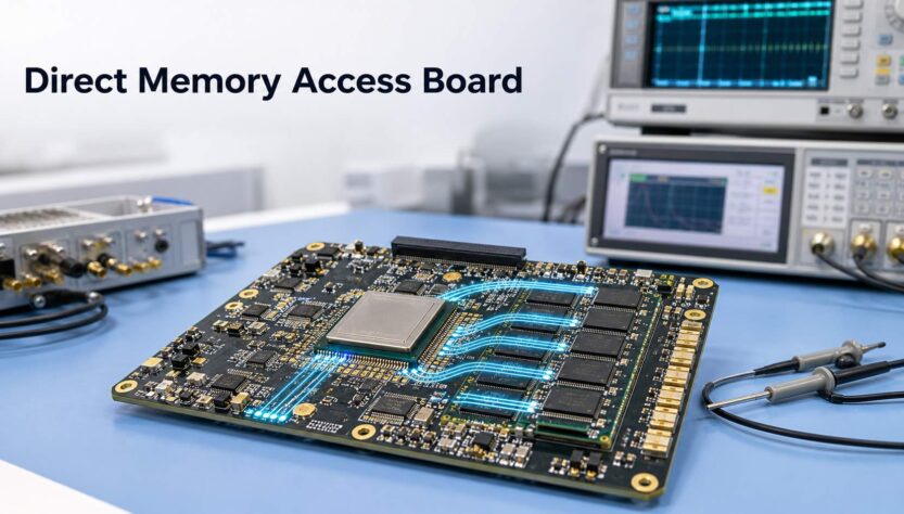
A direct memory access board is used when a system needs fast data movement between memory, processors, peripherals, storage, sensors, or communication interfaces without making the CPU handle every transfer step. In embedded systems, industrial controllers, imaging devices, FPGA platforms, PCIe cards, data acquisition hardware, and test equipment, DMA can help reduce CPU load and improve real-time data handling.
For PCB projects, however, DMA is not only a software or processor feature. A direct memory access board depends on stable signal paths, correct stackup planning, controlled impedance where needed, reliable power distribution, manufacturable BGA routing, clean SMT assembly, and clear testing requirements. EBest Circuit (Best Technology) supports PCB layout manufacturability review, PCB fabrication, component sourcing, PCBA assembly, DFM checks, and production support for custom boards where high-speed data transfer and reliability matter. If you are developing a direct memory access board, FPGA board, PCIe DMA board, or memory-related PCB assembly, send your Gerber files, stackup, BOM, impedance notes, or assembly requirements to sales@bestpcbs.com for an engineering review before production.
What Is a Direct Memory Access Board?
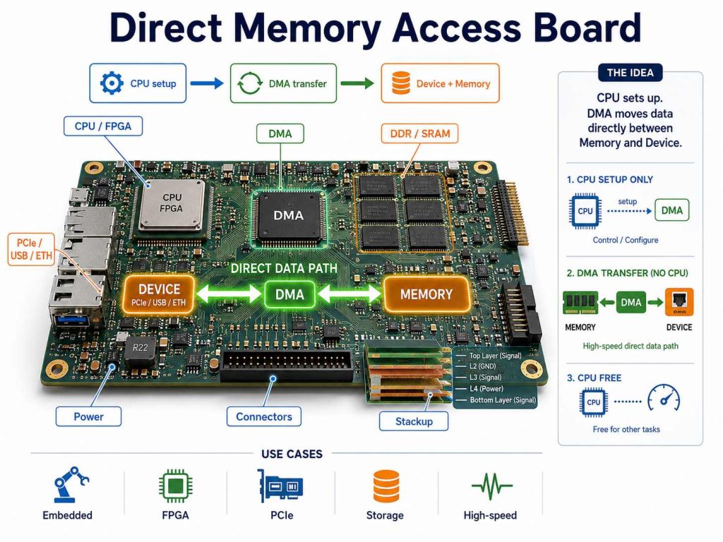
A direct memory access board is a PCB assembly that supports DMA-based data transfer between memory and hardware devices. Instead of asking the CPU to move every byte of data, a DMA controller or DMA-capable peripheral can transfer data directly between memory and a device after the CPU sets up the transfer.
In real hardware, a direct memory access board may include:
| Part | Role on the Board |
|---|---|
| MCU, MPU, CPU, or FPGA | Controls or coordinates the system |
| DMA controller | Manages data transfer without constant CPU involvement |
| Memory devices | DDR, SRAM, flash, eMMC, or other storage |
| High-speed interface | PCIe, USB, Ethernet, MIPI, LVDS, or parallel bus |
| Power circuit | Supports stable operation during high-speed transfer |
| PCB stackup | Provides signal reference planes and routing structure |
| Connectors | Link the board to sensors, displays, host systems, or modules |
A simple embedded board may use DMA inside a microcontroller. A more complex board may use an FPGA, processor, DDR memory, PCIe interface, and external storage. The PCB requirements become more demanding as speed, density, and interface complexity increase.
Direct Memory Access Board vs DMA Card
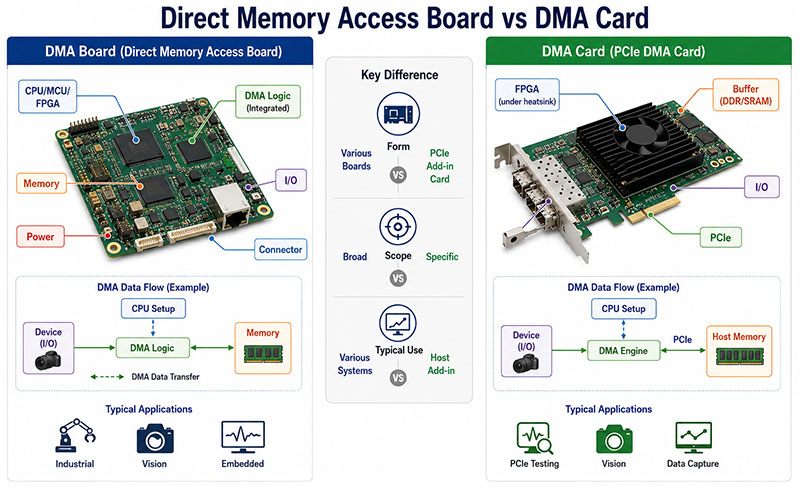
A direct memory access board and a DMA card are related, but they are not always the same thing.
- A direct memory access board is a broader term. It can refer to any PCB or PCBA that uses DMA in an embedded, industrial, computing, imaging, or communication system. It may be a custom controller board, sensor board, FPGA board, processor board, storage interface board, or test board.
- A DMA card usually refers to an add-in card, often using PCIe, that connects to a host system and performs DMA-based transfer. In legitimate engineering applications, a PCIe DMA board can be used for data acquisition, high-speed testing, FPGA development, machine vision, storage acceleration, or laboratory equipment.
The important point is intent and application. This article discusses authorized embedded hardware and PCB manufacturing. It is not a guide to bypassing system security or accessing memory without permission.
How Direct Memory Access Works on a PCB Board
On a PCB board, DMA works through a combination of hardware, memory, bus architecture, and software configuration.
A typical process looks like this:
| Step | What Happens |
|---|---|
| 1 | The CPU configures the DMA transfer |
| 2 | The DMA controller receives source, destination, and data length |
| 3 | The peripheral or memory interface starts the transfer |
| 4 | Data moves without constant CPU copying |
| 5 | The CPU receives an interrupt or status signal when done |
For example, an image sensor may send data to memory through a camera interface. An FPGA may move captured data into DDR memory. A PCIe board may transfer data between onboard memory and a host system. A microcontroller may move ADC data into RAM while the CPU handles other tasks.
From a PCB point of view, the key issue is not only whether DMA exists in the chip. The board must support the electrical and mechanical requirements of the data path. If the memory bus, clock line, differential pair, power rail, or connector layout is unstable, the DMA feature cannot perform reliably.
Key Components in a Direct Memory Access Board
A direct memory access board is usually built around several functional blocks.
Processor or FPGA
- This is the main control device. It may be an MCU, MPU, SoC, CPU, or FPGA. In high-speed projects, BGA packages are common, which makes fanout routing, via selection, and layer planning important.
Memory
- Memory may include DDR, SRAM, NOR flash, NAND flash, eMMC, or external storage. DDR and high-speed memory interfaces often require controlled routing rules, length matching, reference planes, and careful power integrity.
DMA-capable interface
- The board may use PCIe, USB, Ethernet, MIPI CSI, LVDS, SPI, QSPI, parallel bus, or other interfaces. Each interface has different PCB layout and manufacturing requirements.
Power and grounding
- DMA transfer can create active current demand. Stable power rails, decoupling placement, ground reference, and return paths affect signal stability.
Connectors and mechanical structure
- Many direct memory access board projects connect to cameras, sensors, host computers, displays, storage modules, or test fixtures. Connector placement, board thickness, outline tolerance, and assembly clearance should be checked early.
PCIe DMA Board and Embedded DMA Applications
A PCIe DMA board is one of the common board-level applications of DMA. PCIe allows high-speed communication between a custom board and a host system. In engineering use, PCIe DMA can support high-bandwidth data transfer for FPGA platforms, imaging systems, test instruments, communication hardware, and industrial data acquisition.
Embedded DMA applications can also appear in smaller systems. A microcontroller may use DMA to move ADC data into memory. A camera module may use DMA to move image data. A motor controller may use DMA to handle real-time sampling. A display board may use DMA to refresh screen data more efficiently.
Common applications include:
| Application | Why DMA Matters |
|---|---|
| Machine vision | Moves image data quickly |
| Data acquisition | Handles continuous sampling |
| FPGA development | Transfers large data blocks |
| Industrial control | Reduces CPU workload |
| Storage interface | Improves data movement |
| Test equipment | Supports repeatable high-speed capture |
For these projects, PCB manufacturing is part of performance. A good chip selection cannot fix poor routing, weak stackup planning, or unstable assembly quality.
Direct Memory Access Board vs CPU-Controlled Data Transfer
The main advantage of DMA is efficiency. In CPU-controlled transfer, the processor spends time reading data from one place and writing it to another. This can be acceptable for low-speed tasks, but it becomes inefficient when data volume is large or timing is strict.
With DMA, the CPU sets up the transfer and then does other work while the DMA controller handles the movement. This can improve system responsiveness and reduce CPU loading.
| Transfer Method | Best For | Limitation |
|---|---|---|
| CPU-controlled transfer | Simple, low-speed tasks | Uses CPU time |
| DMA transfer | High-speed or repeated data movement | Needs correct hardware and configuration |
On the PCB side, DMA transfer often means the board must support faster interfaces, cleaner signal paths, and better power stability. This is why layout and manufacturability review are important before production.
Can a Direct Memory Access Board Access Flash Memory Directly?
A direct memory access board can access flash memory directly only when the hardware architecture supports it. This depends on the processor, controller, memory type, bus interface, and firmware configuration.
For example, flash memory may be connected through SPI, QSPI, parallel NOR, NAND, eMMC, or another storage interface. In some systems, DMA can move data between flash and RAM through a memory controller or peripheral interface. In other systems, flash access must go through a specific controller, driver, or protocol.
So the better question is not simply “how to access flash memory directly on board?” The real engineering question is:
Can the selected processor, memory interface, PCB layout, and firmware plan support the required flash transfer speed and reliability?
For PCB manufacturing, the important checks include:
| Checkpoint | Why It Matters |
|---|---|
| Flash package | Affects pad design and assembly |
| Interface type | Defines routing and signal rules |
| Clock speed | Affects impedance and signal quality |
| Trace length | Affects timing margin |
| Power stability | Affects read/write reliability |
| Test access | Helps validation and debugging |
EBest Circuit can review Gerber files, stackup, assembly files, and DFM points for the PCB and PCBA side, but firmware-level flash access logic should be handled by the customer’s embedded software or system design team.
PCB Layout and Manufacturing Considerations for Direct Memory Access Boards
For a direct memory access board, PCB layout and manufacturing decisions can directly affect performance and yield. This section focuses on the board-level work that belongs to PCB layout, fabrication, and PCBA support.
Stackup and impedance
- If the board includes PCIe, DDR, USB, Ethernet, MIPI, LVDS, or other high-speed signals, the stackup should be reviewed before routing and production. Controlled impedance may be required for differential pairs or single-ended traces.
BGA and fine-pitch routing
- Many DMA-related boards use FPGAs, processors, memory chips, or high-density connectors. If BGA pitch is small, the project may need HDI, microvias, via-in-pad, resin plug, or additional layers.
Return path and reference planes
- High-speed signals need stable reference planes. Poor return path control can create noise, EMI issues, timing errors, and unstable data transfer.
Power integrity
- DMA transfer can involve fast data movement and active memory access. Power rails should have proper copper distribution, decoupling placement, and ground planning.
Thermal and assembly review
- Processors, FPGAs, memory, and power ICs may generate heat. The layout should leave enough room for assembly, inspection, thermal relief, and rework when needed.
DFM before production
- Before manufacturing, EBest Circuit can check drill size, annular ring, copper clearance, solder mask bridge, impedance notes, panelization, surface finish, and assembly risks. This helps reduce problems before the board reaches fabrication or SMT.
How to Choose a PCB Manufacturer for a Direct Memory Access Board
A direct memory access board is usually not the best project for choosing a supplier only by the lowest online price. The board may involve high-speed signals, BGA devices, impedance requirements, memory routing, tight assembly needs, and test documentation.
A practical supplier should be able to support:
| Requirement | What to Check |
|---|---|
| PCB fabrication | Layer count, copper, HDI, impedance |
| PCBA assembly | BGA, fine pitch, connectors, inspection |
| DFM review | Manufacturing risks before production |
| Component sourcing | BOM risk, alternatives, lead time |
| Testing support | AOI, X-ray, functional test coordination |
| Documentation | Reports, stackup, impedance, inspection notes |
EBest Circuit (Best Technology) supports one-stop PCB and PCBA service for custom boards, including PCB fabrication, component sourcing, PCB SMT assembly, DFM review, BOM optimization support, and testing coordination. For DMA board projects, our engineering team can help review manufacturability, stackup feasibility, impedance requirements, assembly risks, and production documentation before the project moves forward.
This does not replace the customer’s system design, firmware design, or DMA architecture work. It helps make sure the physical board can be manufactured and assembled reliably.
Direct Memory Access Board Manufacturing Case Example
A German customer developed an FPGA-based industrial image acquisition board for a machine vision system. Because the board needed stable high-speed data transfer between the FPGA, memory, and host interface, the project required tight control of HDI fabrication, impedance, BGA reliability, and SMT readiness.
Project Snapshot
- Customer: Germany
- Application: Industrial machine vision
- Board type: 8L HDI FR4 PCB
- Material / thickness: Tg170, 0.97mm
- Copper: 0.5oz
- Via structure: L1-L2 blind vias, L2-L7 buried vias, L7-L8 blind vias
- Minimum via: 0.10mm
- BGA area: Via-in-pad with resin plugging and plated flat surface
- Surface finish: ENIG, 1u” gold
- Assembly support: Panel delivery with 3 fiducial Mark points
- Report: Impedance test report required
Main challenge
This direct memory access board had several impedance requirements, including 50 ohm single-ended, 90 ohm differential, and 100 ohm differential structures on different signal layers. The BGA area also required resin-filled via-in-pad, which made HDI process control and SMT reliability especially important.
EBest Circuit solution
- Reviewed the HDI stackup before production
- Checked impedance feasibility against the 0.97mm board thickness
- Confirmed key impedance structures and raised EQ where needed
- Controlled 0.10mm microvia fabrication and buried/blind via quality
- Managed BGA via-in-pad resin plugging and plating flatness
- Added 3 panel Mark points to support accurate SMT alignment
- Provided impedance testing and report for customer validation
Customer value
For the customer, this was not just an 8-layer HDI board order. EBest Circuit helped control the board-level risks that mattered most: signal integrity, HDI manufacturability, BGA assembly reliability, SMT preparation, and production documentation. This made the FPGA image acquisition board easier to move from engineering files to a reliable PCB assembly.
FAQs about Direct Memory Access Board
1. What is a direct memory access board?
A direct memory access board is a PCB or PCBA that supports DMA-based data movement between memory and hardware devices. It may use an MCU, CPU, FPGA, DMA controller, memory chip, PCIe interface, or other high-speed peripherals.
2. Is a DMA card the same as a direct memory access board?
Not always. A DMA card usually refers to an add-in card, often PCIe-based. A direct memory access board is broader and can include embedded controller boards, FPGA boards, camera processing boards, storage boards, and industrial control boards.
3. Can a direct memory access board access flash memory directly?
Only if the hardware architecture supports it. Flash access depends on the memory type, controller, bus interface, firmware, and PCB layout. DMA may help move data, but it does not automatically bypass the required memory controller or protocol.
4. What PCB layout issues matter most for a direct memory access board?
The main layout issues include stackup, impedance, high-speed routing, BGA fanout, reference planes, power integrity, via structure, connector placement, thermal control, and DFM review.
5. Does EBest Circuit design the full DMA system?
EBest Circuit mainly supports PCB layout manufacturability review, PCB fabrication, component sourcing, PCBA assembly, DFM, and testing coordination. Full system architecture, firmware, driver development, and DMA controller logic should be handled by the customer’s engineering team.
In conclusion, if you are working on a direct memory access board, PCIe DMA board, FPGA board, embedded controller board, or memory-related PCB assembly, the best time to check manufacturability is before production starts. Pls feel free to send your Gerber files, stackup, BOM, assembly drawings, impedance notes, or project requirements to sales@bestpcbs.com. EBest Circuit’s engineering team can help review the PCB and PCBA manufacturing path so your board moves from design files to production with fewer avoidable risks.
Tags: Direct Memory Access Board, DMA board, DMA Card
PakarPBN
A Private Blog Network (PBN) is a collection of websites that are controlled by a single individual or organization and used primarily to build backlinks to a “money site” in order to influence its ranking in search engines such as Google. The core idea behind a PBN is based on the importance of backlinks in Google’s ranking algorithm. Since Google views backlinks as signals of authority and trust, some website owners attempt to artificially create these signals through a controlled network of sites.
In a typical PBN setup, the owner acquires expired or aged domains that already have existing authority, backlinks, and history. These domains are rebuilt with new content and hosted separately, often using different IP addresses, hosting providers, themes, and ownership details to make them appear unrelated. Within the content published on these sites, links are strategically placed that point to the main website the owner wants to rank higher. By doing this, the owner attempts to pass link equity (also known as “link juice”) from the PBN sites to the target website.
The purpose of a PBN is to give the impression that the target website is naturally earning links from multiple independent sources. If done effectively, this can temporarily improve keyword rankings, increase organic visibility, and drive more traffic from search results.