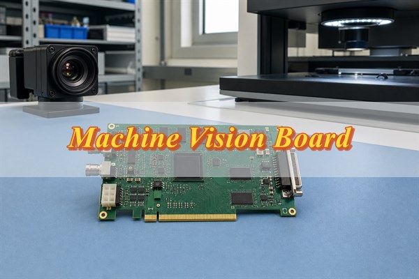
A machine vision board must acquire every required frame, preserve trigger timing, process the image within the cycle time, and deliver a valid result under sustained industrial load. That outcome depends on the complete path: camera interface, FPGA/GPU/NPU partitioning, DDR buffering, PCIe or network transfer, power, heat, PCB construction, assembly, and functional test.
What Is a Machine Vision Board for Industrial Image Processing?
A machine vision board is the deterministic hardware path between image capture and a machine decision. It accepts one or more camera streams, associates frames with triggers or timestamps, performs preprocessing or inference, and sends results to a host, PLC, robot controller, or motion system.
The board may be a PCIe frame grabber, an embedded controller, or a custom PCBA inside an inspection machine. Its functional boundary is wider than a camera PCB module, which mainly supports the sensor and local imaging electronics, and different from an IP camera PCB, which is organized around network video capture and delivery. A machine vision board commonly owns frame buffering, deterministic I/O, image processing, diagnostics, and host communication.
For AOI, robotic guidance, metrology, sorting, and multi-camera inspection, image quality is only one acceptance item. The specification must also define maximum trigger-to-result latency, permitted camera skew, dropped-frame behavior, recovery time, operating temperature, output safety state, and the exact revision of firmware and AI models used for acceptance.
How Should You Choose FPGA, GPU, or NPU Processing for a Machine Vision Board?
Select compute by assigning each pipeline stage to the device that can meet its worst-case latency, throughput, power, and software-support requirement. Peak TOPS does not prove that a board can ingest every camera, move intermediate data through memory, and return a decision before the machine cycle expires.
| Processing option | Best use | Board design impact |
| FPGA | Sensor control, protocol conversion, line-rate filtering, pixel alignment, and deterministic trigger logic | Multiple clock domains, high-speed I/O banks, configuration memory, timing closure, and tightly sequenced rails |
| GPU | Flexible image algorithms, large parallel workloads, and models that change during product development | High DDR traffic, substantial core power, heat spreading, and dependency on drivers and software libraries |
| NPU | Supported neural-network inference where performance per watt is the main constraint | Operator and precision compatibility, model conversion, accelerator memory movement, and fallback planning |
| Hybrid | FPGA acquisition and preprocessing followed by GPU or NPU analytics | Explicit buffer ownership, inter-device bandwidth, timestamp transfer, boot order, and error recovery |
FPGA-based image processing is useful when parallel, data-heavy front-end operations must run with stable latency. A practical hybrid design can perform debayering, region extraction, line buffering, or geometric correction in FPGA logic and send only the required frames or features to a GPU or NPU. This reduces downstream traffic, but it also creates a new verification boundary: the design must prove how metadata, timestamps, frame IDs, and error flags move with the processed data.
Before fixing the processor, benchmark the intended pipeline with the actual resolution, bit depth, camera count, model, precision mode, and temperature target. Record average and worst-case latency, memory usage, accelerator utilization, and throttling behavior. If a required AI operator is unsupported, model conversion changes accuracy, or performance collapses after thermal saturation, the board architecture is not ready for release.
Which Camera Interfaces Belong on an Industrial Machine Vision Board?
Use MIPI CSI-2 for nearby embedded sensors, GigE Vision for distributed industrial cameras, and USB3 Vision for high-throughput host-connected cameras where cable routing and service access are controlled. The choice must follow physical placement, sustained payload, synchronization method, connector life, field replacement, and the software ecosystem.
| Interface | Suitable architecture | PCB priority | Acceptance focus |
| MIPI CSI-2 | Image sensor mounted on the same assembly or connected through a short controlled interconnect | Continuous reference planes, controlled differential geometry, short lane transitions, and correct sensor rail sequencing | Lane mapping, bit depth, frame start/end integrity, clock behavior, and error counters |
| GigE Vision | Remote or distributed cameras that benefit from Ethernet infrastructure and field-serviceable cabling | PHY and magnetics placement, return-path isolation, connector shielding, surge/ESD strategy, and network power planning when applicable | Sustained packet delivery, timestamp behavior, packet loss, recovery, and multi-camera traffic contention |
| USB3 Vision | High-data-rate cameras located near the host or embedded controller | SuperSpeed channel loss, connector footprint, ESD parasitics, power integrity, and cable retention | Enumeration, sustained transfer, reconnect recovery, host-controller loading, and dropped-frame counters |
Do not treat a common software layer as proof that the electrical links are interchangeable. Each interface needs its own impedance plan, connector model, protection components, power budget, compliance test, and error-injection method. If one board supports several camera types, isolate their clock and bandwidth domains and define which device owns triggers, timestamps, buffers, and recovery.
How Do Pixel Rate, DDR Bandwidth, and PCIe Traffic Shape the Board Architecture?
Calculate sustained traffic separately for camera input, every DDR read/write pass, accelerator transfer, and host output. The basic raw payload is active width x active height x frame rate x bits per pixel x camera count. Add protocol, alignment, blanking, metadata, and retry allowances only after the raw stream is visible.
As an illustrative calculation, a 1920 x 1080 stream at 60 frames per second and 10 bits per pixel carries 1,244,160,000 raw bits per second, or 155.52 MB/s before overhead. Four such cameras produce 622.08 MB/s. If the pipeline writes raw frames to DDR, reads them for processing, writes an intermediate result, reads it again for inference, and sends the output to a host, total memory traffic can be several times the incoming payload.
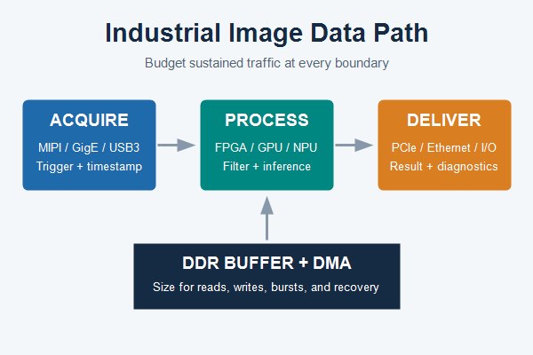
Build a bandwidth worksheet with one row for each transfer, its direction, payload, burst size, duty cycle, and simultaneous operating condition. Size DDR from the sum of competing reads and writes, not the camera stream alone. Size frame buffers from the longest permitted backpressure or recovery interval, then define what happens when the buffer fills: block acquisition, drop the newest frame, drop the oldest frame, or flag the inspection cycle invalid.
PCIe lane rate is not application payload. Encoding, packets, transaction size, DMA descriptors, cache behavior, host contention, and software scheduling reduce usable throughput. The acceptance test should therefore measure sustained end-to-end traffic with all cameras active and retain margin for bursts, temperature-related throttling, error recovery, and future firmware growth.
What PCB Layout Risks Threaten High-Speed Image Data Integrity?
The dominant risks are discontinuities in impedance and return current, not simply long traces. A nominally matched differential pair can still fail at a connector breakout, layer transition, via stub, split reference plane, oversized ESD pad, or noisy receiver reference.
- Lock the stack-up: obtain the fabricator’s dielectric thicknesses, copper weights, material family, and impedance geometry before high-speed placement is frozen.
- Preserve return paths: keep each lane over a continuous reference plane and place nearby return vias when signals change reference layers.
- Control transitions: include connector fields, AC-coupling pads, ESD devices, test points, and BGA escape vias in the channel model.
- Separate noise sources: keep switch nodes, motor or strobe currents, high-current connector returns, and fast clocks away from camera analog rails and sensitive references.
- Verify the real channel: use the transmitter, receiver, connector, via, and material models required by the component vendors; do not apply one universal length or skew limit to every interface.
Dense FPGA, processor, or DDR fan-out may require an HDI PCB structure, but microvias cannot correct a poor topology. Review via-in-pad requirements, capture-pad size, sequential lamination, escape layers, reference changes, and inspection access together. Where margin is limited, run pre-layout and post-layout signal-integrity checks against the actual stack-up.
How Should Power Integrity, Heat, and Mechanical Constraints Be Reviewed?
Power, thermal, and mechanical reviews must use the same worst-case operating mode because rail droop, throttling, and board strain can produce identical intermittent image faults. Create a rail budget for every processor, FPGA bank, DDR rail, camera supply, PHY, illumination control, and auxiliary I/O.
- Define rail behavior: record nominal voltage, tolerance, steady current, transient current, sequencing, soft-start, reset relationship, monitoring, and shutdown state.
- Design the PDN: select bulk and high-frequency decoupling from the device impedance target and package model, then check plane spreading and via inductance.
- Test sustained heat: run the maximum camera count and processing load until temperatures stabilize; observe junction estimates, regulator temperatures, clock reduction, and frame latency.
- Close mechanical clearances: check heat-sink attachment, connector mating space, cable bend and retention, mounting-hole stress, enclosure airflow, and probe access.
A thermal solution is acceptable only if the board meets timing and image-throughput limits at the specified enclosure temperature. Likewise, a mechanical drawing is incomplete if it omits connector keep-outs, camera harness direction, heat-sink loading, or the tolerance stack between the PCB, standoffs, enclosure, and optical assembly.
How Is a Machine Vision Board Manufactured and Assembled?
Manufacturing should begin with a stack-up and assembly-risk review tied to the exact board revision. High-speed routing, fine-pitch BGA escape, blind or buried vias, heavy connectors, and thermal pads affect fabrication, solder-paste design, inspection, rework, and test-fixture access.
The following values come from EBest Circuit’s current English FR-4 capability workbook. General values are starting points for review; special-process values require confirmation against the final stack-up, panel, copper distribution, via structure, and reliability requirements.
- FR-4 layer count: the general capability is 1-10 layers, with high-Tg material required for 8 layers and above. Designs from 10-32 layers require special-process review.
- Laser blind or buried vias: the general capability is 0.10 mm. The final review must confirm capture pads, via fill, and the sequential-lamination structure.
- Minimum finished hole: the general capability is 0.20 mm. A 0.15 mm finished hole requires special-process review.
- Through-hole aspect ratio: the general capability is 8:1. A ratio up to 10:1 requires special-process review.
- 1 oz line and space: the general capability for inner or outer layers is 4/4 mil. A 3/3 mil design requires special-process review.
- ENIG thickness: the listed range is 0.025-0.125 um for gold and 3-8 um for nickel. Wear, contact, or bonding requirements must be confirmed separately.
Before assembly, classify bottom-terminated components, fine-pitch BGAs, large exposed pads, moisture-sensitive packages, press-fit parts, high-mass connectors, and devices that require programming. Paste apertures and reflow profiling should address voiding and thermal imbalance without creating solder starvation. AOI verifies visible placement, polarity, and joints; X-ray supports hidden-joint inspection. Neither replaces electrical and functional testing of the image path.
How Should Trigger, Synchronization, and Functional Testing Be Validated?
Validation must correlate the commanded trigger, actual frame, hardware timestamp, processed result, and system output under sustained load. A live image proves only that part of the path is operating; it does not prove that the correct frame belongs to the correct machine event.
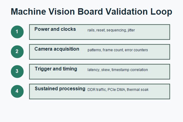
- Verify power and boot: test cold starts, warm restarts, brownouts, and maximum-load transitions. Record rail timing, reset release, clocks, boot logs, and current profiles; boot loops, unstable links, corrupted configuration, or abnormal current are failures.
- Confirm image acquisition: run known camera patterns through every supported format, bit depth, and lane configuration. Check frame IDs, line length, pixel order, and link-error counters for lane swaps, truncation, corrupted lines, color errors, or missing frames.
- Measure trigger and synchronization: apply timed trigger and encoder patterns while all required cameras are active. Compare trigger-to-exposure latency, inter-camera skew, hardware timestamps, and missed-event counts; drifting skew, duplicate events, lost triggers, or incorrect frame association must fail.
- Stress sustained processing: operate at the maximum camera count, frame rate, algorithm load, and host-transfer rate until temperature stabilizes. Monitor latency distribution, buffer level, DMA counters, temperature, and throttling; backlog growth, dropped frames, timeouts, or stale results show insufficient margin.
- Challenge fault recovery: introduce controlled cable interruptions, invalid packets, camera resets, and host restarts. Verify the reported error, safe output state, recovery time, restored counters, and log record; silent corruption, unsafe outputs, mixed frame IDs, or manual-only recovery are unacceptable.
- Control production testing: use a fixture that generates repeatable inputs and reads machine-verifiable outputs. Lock firmware and model versions, camera or pattern-generator settings, instrument setup, numeric limits, timeout rules, and failure codes, then retain results by unit serial number. Golden samples can monitor fixture stability but do not replace calibrated limits and revision control.
What DFM Checks Are Required Before Machine Vision Board Production?
A release-ready DFM review closes fabrication, assembly, test, and configuration risks against one controlled data package. The output should be an issue list with an owner, disposition, affected revision, and evidence that the approved change reached the final files.
- Stack-up and impedance: confirm material family, finished thickness, copper weights, controlled structures, coupons, and tolerance assumptions.
- Drill and via plan: check finished holes, aspect ratios, blind/buried-via spans, via fill, backdrill when required, annular rings, and sequential lamination.
- Assembly access: review paste apertures, thermal pads, polarity, component spacing, rework access, support tooling, press-fit loads, and selective-solder constraints.
- Mechanical closure: match the PCB outline, connector mating direction, keep-outs, mounting holes, heat sink, enclosure, and cable drawings.
- Test coverage: provide accessible points for rails, resets, clocks, trigger I/O, programming, debug, boundary scan, and functional fixtures.
- Configuration control: freeze manufacturer part numbers, approved substitutes, firmware, FPGA images, AI models, programming instructions, and acceptance limits by revision.
The production package should include Gerber or ODB++, drill and stack-up data, schematic PDF, BOM, centroid data, assembly drawings, impedance requirements, mechanical files, programming files, and test instructions. Missing information should remain an open issue; it should not be replaced with an assumed factory default.
Why Choose EBest Circuit for Machine Vision Board Manufacturing?
Choose EBest Circuit to turn a complex machine vision board design into a clearer, lower-risk manufacturing release. Instead of treating fabrication, assembly, component sourcing, programming, and testing as separate activities, the review connects them around the camera-to-result data path that your equipment must sustain.
- Find production risks earlier: high-speed stack-up, BGA escape, DDR and PCIe routing, thermal pads, connector loads, and test access can be reviewed before tooling and component purchasing make changes more costly.
- Reduce avoidable revision cycles: fabrication data, BOM, placement files, mechanical constraints, firmware, and acceptance limits are checked as one controlled package, helping prevent mismatched revisions and missing production instructions.
- Protect schedule and sourcing decisions: special-process features and component constraints are identified for engineering confirmation before they become late quotation, material, assembly, or test surprises.
- Make quality requirements measurable: camera formats, frame rates, trigger timing, operating temperature, programming steps, and functional limits can be translated into inspection and test requirements for the finished PCBA.
Send your Gerber or ODB++, schematic, BOM, stack-up target, impedance requirements, assembly files, camera specifications, firmware, and test limits. EBest Circuit can use that package to prepare a more relevant manufacturing review and quotation for your machine vision board, with special-process items clearly identified for confirmation.
FAQs About Machine Vision Boards
Q1: What Does a Frame Grabber Do in a Machine Vision System?
A1: A frame grabber receives camera data and presents complete, identified frames to a host or processing pipeline. Depending on the design, it can also control triggers, buffer bursts, convert formats, timestamp events, and move data through DMA.
Q2: How Does Machine Vision Work in an Industrial Inspection System?
A2: Repeatable optics, timing, and part presentation are required while the system controls lighting and exposure, acquires an image, applies a defined inspection pipeline, and sends a result to the machine controller.
Q3: Are FPGAs Still Relevant to Industrial Machine Vision?
A3: Yes, particularly for deterministic acquisition and parallel preprocessing. An FPGA is optional when another device can meet every interface, latency, trigger, power, and software requirement without it.
Q4: What Are Hardware Timestamps Used for in Machine Vision?
A4: Hardware timestamps correlate frames, triggers, encoders, lighting pulses, and motion in a defined clock domain without relying solely on nondeterministic software time.
Q5: What Causes Dropped Frames in a Machine Vision Pipeline?
A5: Frame IDs, buffer levels, timestamps, and boundary-specific error counters locate the failing stage. Causes can include signal errors, insufficient buffers, blocked DMA, host contention, trigger faults, or thermal throttling.
Q6: What Does AOI Test on an Assembled Machine Vision PCB?
A6: AOI checks visible component presence, polarity, placement, and accessible solder joints. It does not verify hidden BGA joints or functional image processing, so X-ray, electrical test, and functional test address different risks.
Q7: What Does PCB Functional Testing Verify?
A7: Functional testing applies controlled inputs and checks defined electrical and system outputs. For a vision board, it can cover boot, rails, clocks, acquisition, memory traffic, host transfer, trigger timing, error reporting, and recovery.
Q8: What Types of Machine Vision Systems Use Custom Processing Boards?
A8: Custom boards suit systems with requirements that commercial hardware cannot meet. Compare form factor, interface mix, latency, environmental limits, machine I/O, development, certification, fixture, lifecycle, and maintenance costs.
Q9: What Are the Main Stages of Machine Vision Processing?
A9: The main stages are acquisition, preprocessing, feature extraction or inference, decision logic, and result communication. Buffering, timestamps, diagnostics, and recovery keep those stages traceable during production use.
Q10: Is Machine Vision the Same as Artificial Intelligence?
A10: No. Machine vision is the complete industrial imaging system, while AI is one possible processing method. Many inspection tasks use geometry, filtering, matching, measurement, or deterministic rules without a neural network.
Conclusion
A reliable machine vision board is specified and verified as one data, timing, power, thermal, manufacturing, and test system. Interface speed or accelerator performance alone cannot guarantee deterministic inspection. The board must sustain every active stream, preserve frame identity, control triggers, tolerate real operating temperature, and produce observable pass/fail evidence.
To request a machine vision board review, email sales@bestpcbs.com with Gerber or ODB++, schematic, BOM, quantity, stack-up and impedance requirements, assembly files, camera formats, bandwidth calculations, trigger specification, mechanical constraints, firmware or programming files, and functional-test limits.
Tags: machine vision board, machine vision FPGA, machine vision PCB, machine vision processing
PakarPBN
A Private Blog Network (PBN) is a collection of websites that are controlled by a single individual or organization and used primarily to build backlinks to a “money site” in order to influence its ranking in search engines such as Google. The core idea behind a PBN is based on the importance of backlinks in Google’s ranking algorithm. Since Google views backlinks as signals of authority and trust, some website owners attempt to artificially create these signals through a controlled network of sites.
In a typical PBN setup, the owner acquires expired or aged domains that already have existing authority, backlinks, and history. These domains are rebuilt with new content and hosted separately, often using different IP addresses, hosting providers, themes, and ownership details to make them appear unrelated. Within the content published on these sites, links are strategically placed that point to the main website the owner wants to rank higher. By doing this, the owner attempts to pass link equity (also known as “link juice”) from the PBN sites to the target website.
The purpose of a PBN is to give the impression that the target website is naturally earning links from multiple independent sources. If done effectively, this can temporarily improve keyword rankings, increase organic visibility, and drive more traffic from search results.