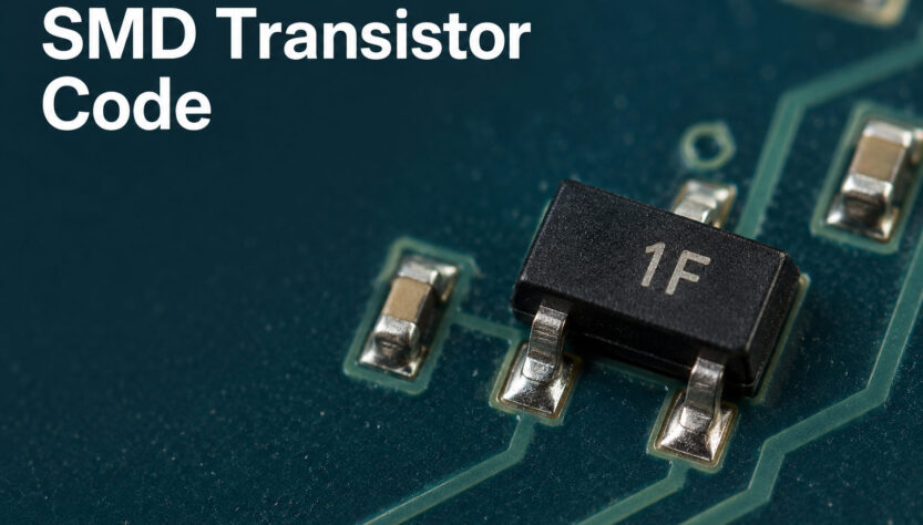
An SMD transistor code is the short marking on a surface-mount transistor, used to look up its identity when the package cannot carry a full part number. A code match gives you a candidate; the manufacturer, package and pinout determine whether that candidate fits the device on your board. This guide provides a marking chart and a practical way to move from a tiny top mark to a defensible identification and replacement choice.
EBest Circuit (Best Technology) supports component sourcing and PCB assembly using manufacturer part numbers, package requirements and approved alternatives. That connection between sourcing and assembly helps you carry a confirmed component choice into the BOM and board build. For sourcing availability or a PCBA quotation based on your identified transistor, contact sales@bestpcbs.com.
What Is an SMD Transistor Code?
An SMD transistor code is a manufacturer-assigned package marking. It may contain letters, numbers or both, with additional characters identifying production information. It is not a universal encoding system that lets you calculate transistor ratings from the characters alone.
Three different identifiers can appear in the same identification task:
- Package marking: the characters printed or laser-marked on the component, such as the device-code portion
1F. - Manufacturer part number: the transistor identity used to find its datasheet, such as Nexperia BC847B. Ordering suffixes may also distinguish packing or other supply options.
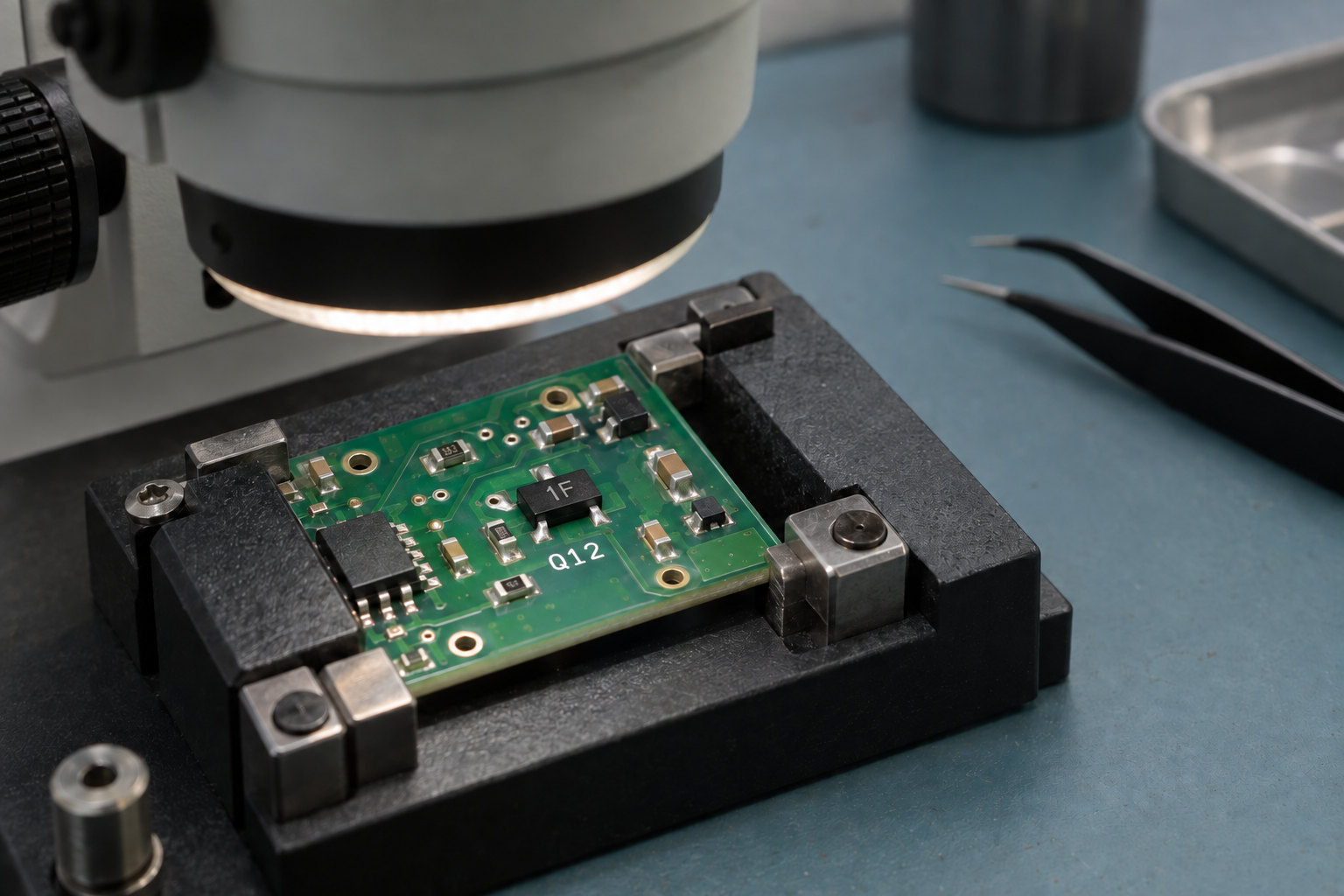
- PCB reference designator: a board location such as Q12, which identifies a position in the schematic and BOM, not a transistor model.
Reading Q12 beside a component therefore tells you where to search in the assembly documents. Reading its top mark helps identify the component itself. If a BOM is available, start with the entry for that board position and revision; a generic code search should not override it without resolving the discrepancy.
SMD Transistor Code Chart: Common Markings and Part Numbers
Use this SMD transistor code chart to find possible matches, then check the complete marking format and package. The entries are manufacturer-specific examples, not a universal or exhaustive code list.
| Device-code portion | Manufacturer | Candidate part number | Type | Package |
|---|---|---|---|---|
| 1H | Nexperia | BC847 | NPN BJT | SOT23 |
| 1E | Nexperia | BC847A | NPN BJT | SOT23 |
| 1F | Nexperia | BC847B | NPN BJT | SOT23 |
| 1G | Nexperia | BC847C | NPN BJT | SOT23 |
| 7A | Nexperia | MMBT3904 | NPN BJT | SOT23 |
| 3E | Nexperia | BC857A | PNP BJT | SOT23 |
| 3F | Nexperia | BC857B | PNP BJT | SOT23 |
In these Nexperia marking tables, the code is followed by %, a placeholder for a manufacturing-site character. For example, 1F% describes a marking format; it does not require a literal percent sign on the device.
The A, B and C suffixes in the BC847 family identify different gain selections. Do not discard that suffix when recording the candidate part number. A package marked 1F is also not automatically BC847B: the table establishes one valid mapping, not exclusive ownership of the code.
Record the result as “candidate manufacturer + complete part number + package.” That gives you something specific to verify instead of a loose two-character purchasing description.
How to Read an SMD Transistor Marking Code
Read the physical marking before trying to interpret it. One mistaken character can send the search toward a different device family.
- Capture the component in place. With the board safely powered down, photograph the top surface, lead arrangement and nearby reference designator. Keep an unedited image so that later contrast adjustments do not replace the original evidence.
- Check orientation and lighting. Inspect the package under magnification with light from more than one angle. Compare ambiguous characters such as 0/O, 1/I and 5/S without assuming which one was intended.
- Transcribe every visible line. Preserve spacing, dots, logos and smaller characters. Note uncertain characters explicitly instead of silently guessing.
- Measure the package. Record lead count, body dimensions and lead spacing. Two three-lead packages can look similar in a photograph while requiring different footprints.
- Separate device and traceability characters using the manufacturer’s marking instructions. Search the full marking first, then a supported device-code portion if the datasheet explains the extra characters.
For example, the % notation in Nexperia’s BC847 marking format tells you why a character may appear after 1F. It does not justify stripping the final character from every three-character transistor marking. Another manufacturer may use all three characters to identify the device.
If the marking is faint, improve lighting and focus before cleaning. Use only a cleaning method compatible with the component and assembly; scraping the package can remove the very information you need.
Why Does One SMD Code Match Different Components?
Short marking codes are reused across manufacturers and component families. Search databases can therefore return several candidates for the same characters, including devices that are not transistors. A three-lead outline alone does not distinguish a BJT, MOSFET, dual diode or small regulator.
Narrow the candidates in the following order:
- Match the physical package. Reject candidates with the wrong lead count, dimensions or lead arrangement. A matching code on a different package is not enough.
- Match the manufacturer and full marking format. Use a readable logo, reel label or BOM manufacturer entry where available. Keep an unknown manufacturer unresolved rather than selecting the first database result.
- Match the internal device type. Check the datasheet symbol: an ordinary transistor, a resistor-equipped transistor and a diode pair can behave differently despite similar packaging.
- Match the board connections. Compare the candidate’s terminals with the schematic and actual pad connections, then perform the relevant electrical cross-check.
Circuit position provides a clue, not proof. A device beside an inductor might participate in switching, sensing or regulation. Its proximity to the inductor does not establish that it is a particular MOSFET.
If two candidates survive these checks, the identity is still unresolved. Use the correct-revision BOM, assembly records, original supplier information or an intact matching assembly to distinguish them. For broader board markings beyond transistors, see our PCB components identification guide.
How to Verify an SMD Transistor Pinout
Verify an SMD transistor pinout against the exact candidate datasheet. The package name describes mechanical geometry; it does not assign one universal electrical function to each lead.
For Nexperia BC847B in SOT23, the pin assignment is:
| Pin number | Terminal | Meaning |
|---|---|---|
| 1 | B | Base |
| 2 | E | Emitter |
| 3 | C | Collector |
First match the datasheet’s package view to the component orientation. A bottom view mirrors a top view, and a rotated component on the PCB changes where the numbered pins appear to the observer. Do not use the direction of the printed text as a universal pin-1 indicator.
Next, compare those numbered terminals with the board nets. For an illustrative low-side NPN switch, the emitter normally connects toward the ground return, the collector to the load, and the base to its drive network. If the candidate assignment places the base on the load pad, recheck orientation, the schematic and the candidate identity before fitting a replacement.
Trace hidden connections with the unpowered board’s schematic and appropriate continuity checks. A trace disappearing into a via does not end there. The transistor pinout guide covers the wider terminal conventions; here the goal is to confirm that the code candidate matches this specific footprint and circuit.
How Do I Check My SMD Transistor?
A multimeter can reveal basic junction behavior and possible shorts or opens. It cannot authenticate a transistor part number or establish its full voltage, current, gain and switching performance.
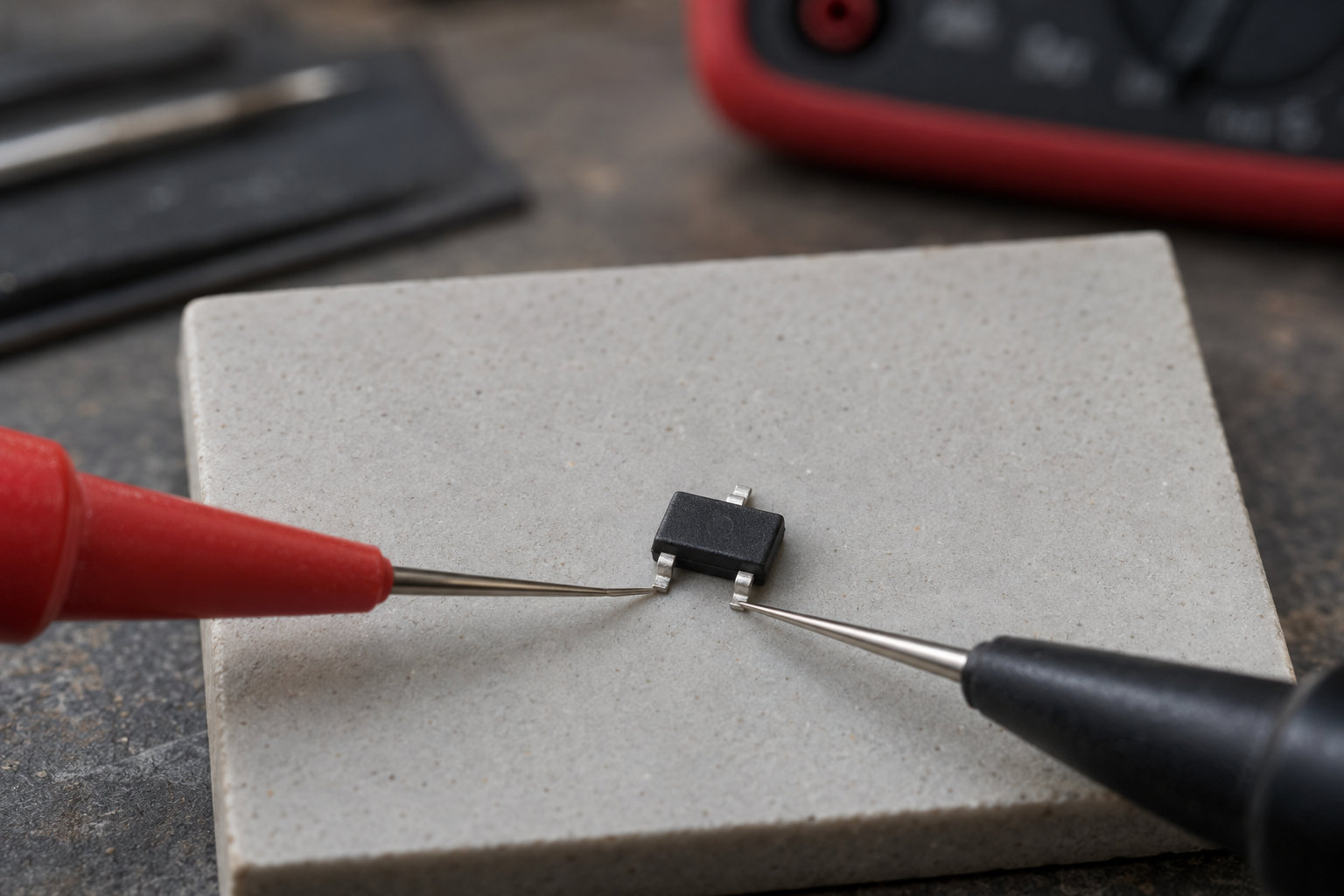
Disconnect all power sources, discharge stored energy safely, and verify that no voltage remains before using resistance or diode mode. Mains-connected and high-energy assemblies require appropriate training and equipment. Do not treat a power switch in the OFF position as proof that the board is safe.
For an ordinary silicon BJT with its pinout established, diode mode can check the base-emitter and base-collector junctions. The table assumes the meter’s red lead is positive in diode mode and the device is isolated sufficiently to avoid parallel circuit paths.
| Candidate type | Forward-bias connection | Reverse-bias connection | Expected basic pattern |
|---|---|---|---|
| NPN | Red on base; black on emitter, then collector | Black on base; red on emitter, then collector | Each junction conducts forward and blocks in reverse |
| PNP | Black on base; red on emitter, then collector | Red on base; black on emitter, then collector | Each junction conducts forward and blocks in reverse |
A forward drop around 0.5–0.8 V is common for a silicon junction, but meter current, temperature and device construction affect the reading. Treat that range as a diagnostic clue, not a universal acceptance limit.
If readings contradict the expected pattern, check probe contact and board paths first. A parallel resistor or another semiconductor can create an apparent conducting path. Where necessary, have a suitably equipped technician isolate or remove the component and repeat the test without damaging its pads.
A persistent near-short in both directions across an isolated junction suggests failure. A persistent open reading in both directions can indicate an open junction, poor contact or an incorrect terminal assumption. Two normal-looking junction readings still do not prove that the transistor works correctly under load, and they do not reliably distinguish collector from emitter by themselves.
Do not apply this simple pattern unchanged to MOSFETs, Darlington devices or resistor-equipped “digital transistors.” Their internal structures require different interpretation. For a MOSFET, identify gate, source and drain first and use a device-appropriate test; the body diode alone does not verify gate control or low on-resistance.
How to Choose a Replacement After Identifying the Transistor
Choose a replacement by the circuit’s operating requirements, not by the top mark. A different code can belong to a suitable alternative, while the same code can belong to an incompatible component.
Work through the selection in this order:
- Establish the required function. Determine whether the device amplifies, switches a load or performs another role. Record the relevant operating voltage, current, drive conditions and temperature range.
- Eliminate structural mismatches. Match BJT versus MOSFET, polarity or channel type, internal resistors or diodes, package dimensions and pin assignment. A part that fits the pads but swaps terminals is not a drop-in replacement.
- Check electrical and thermal limits together. Compare steady-state and transient stresses with the candidate’s ratings and safe operating area where applicable. A headline current rating does not guarantee operation at high voltage or on your board’s copper area.
- Check performance at the available drive. For a switching BJT, compare saturation voltage at the required collector current and available base current. For a MOSFET, compare guaranteed on-resistance at the actual gate-drive voltage, not only its threshold voltage.
- Resolve the application-specific limitation. An amplifier may depend on gain range, leakage, capacitance or noise. A fast switch may be limited by storage time or gate charge. Select for the parameter that controls this circuit rather than assuming a higher headline rating is always better.
- Validate and approve the change. Check the operating circuit, including relevant load and temperature conditions, before releasing an alternative into production. Record the exact manufacturer part number and approved substitution in the BOM.
For example, a MOSFET with an on-resistance guarantee only at 10 V gate drive has not thereby demonstrated the required performance on a 3.3 V drive signal. A threshold below 3.3 V indicates the onset of conduction under specified test conditions, not guaranteed low-resistance operation at the load current.
Similarly, a BJT’s small-signal gain value does not establish its saturation voltage with a limited base drive. Compare the saturation test conditions with the real circuit. If the available base current is lower than the datasheet condition, that saturation-voltage limit cannot simply be carried over.
Once the electrical alternative is approved, EBest Circuit can evaluate sourcing availability and coordinate PCB assembly around the specified part. Keeping the approved identity in the BOM prevents a later purchasing decision from reverting to an ambiguous package code.
FAQs About SMD Transistor Code
Is there a universal SMD transistor code calculator?
No. Transistor package markings do not follow one universal arithmetic rule. A tool described as a calculator usually performs a database lookup. Use its results as candidates and check the manufacturer’s marking information, package and pinout.
Can I use an SMD transistor code PDF to identify a part?
Yes, as a lookup aid. Check whether the PDF identifies manufacturers and packages, and confirm the selected entry against the relevant manufacturer documentation. Older codebooks can omit newer devices or combine several matches under one code.
What should I do if the transistor marking is unreadable?
Start with the board reference designator and the correct-revision BOM or schematic. An intact matching board, original reel label or assembly purchase record can help recover the identity. Package shape and circuit behavior may narrow the possibilities, but they may not recover the exact original part number.
Can a phone photo identify an SMD transistor accurately?
A sharp photo can preserve the marking, logo and lead arrangement for comparison. Include a close-up and a wider view showing the board position. A photo alone usually cannot establish hidden connections, electrical ratings or authenticity, especially when several parts share a marking.
Does a different top mark mean the supplied transistor is counterfeit?
Not by itself. Manufacturer-specific marking formats and traceability characters can differ. Compare the supplied manufacturer’s part number, authorized marking information and purchasing records. If the difference remains unexplained, hold the material for supplier clarification rather than accepting or rejecting it solely by appearance.
If an SMD transistor code lookup has led you to a confirmed part for your next board build, EBest Circuit can help evaluate its supply options and PCB assembly requirements. Contact sales@bestpcbs.com to discuss availability or a PCBA quotation, with engineering-approved alternatives kept separate from unverified code matches.
Tags: SMD Transistor Code, SMD Transistor Code Chart, SMD Transistor Pinout
PakarPBN
A Private Blog Network (PBN) is a collection of websites that are controlled by a single individual or organization and used primarily to build backlinks to a “money site” in order to influence its ranking in search engines such as Google. The core idea behind a PBN is based on the importance of backlinks in Google’s ranking algorithm. Since Google views backlinks as signals of authority and trust, some website owners attempt to artificially create these signals through a controlled network of sites.
In a typical PBN setup, the owner acquires expired or aged domains that already have existing authority, backlinks, and history. These domains are rebuilt with new content and hosted separately, often using different IP addresses, hosting providers, themes, and ownership details to make them appear unrelated. Within the content published on these sites, links are strategically placed that point to the main website the owner wants to rank higher. By doing this, the owner attempts to pass link equity (also known as “link juice”) from the PBN sites to the target website.
The purpose of a PBN is to give the impression that the target website is naturally earning links from multiple independent sources. If done effectively, this can temporarily improve keyword rankings, increase organic visibility, and drive more traffic from search results.